
Datasheet


TMS320F2810, TMS320F2811, TMS320F2812
TMS320C2810, TMS320C2811, TMS320C2812
www.ti.com
SPRS174T –APRIL 2001–REVISED MAY 2012
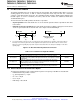
Table 3-16. PLLCR Register Bit Definitions
XRS
BIT(S) NAME TYPE DESCRIPTION
RESET
(1)
15:4 Reserved R = 0 0:0
SYSCLKOUT = (XCLKIN * n)/2, where n is the PLL multiplication
factor.
Bit Value n SYSCLKOUT
0000 PLL Bypassed XCLKIN/2
0001 1 XCLKIN/2
0010 2 XCLKIN
0011 3 XCLKIN * 1.5
0100 4 XCLKIN * 2
0101 5 XCLKIN * 2.5
3:0 DIV R/W 0,0,0,0
0110 6 XCLKIN * 3
0111 7 XCLKIN * 3.5
1000 8 XCLKIN * 4
1001 9 XCLKIN * 4.5
1010 10 XCLKIN * 5
1011 11 Reserved
1100 12 Reserved
1101 13 Reserved
1110 14 Reserved
1111 15 Reserved
(1) The PLLCR register is reset to a known state by the XRS reset line. If a reset is issued by the debugger, the PLL clocking ratio is
not changed.
3.8.1 Loss of Input Clock
In PLL enabled mode, if the input clock XCLKIN or the oscillator clock is removed or absent, the PLL will
still issue a “limp-mode” clock. The limp-mode clock will continue to clock the CPU and peripherals at a
typical frequency of 1–4 MHz. The PLLCR register should have been written to with a non-zero value for
this feature to work.
Normally, when the input clocks are present, the watchdog counter will decrement to initiate a watchdog
reset or WDINT interrupt. However, when the external input clock fails, the watchdog counter will stop
decrementing (that is, the watchdog counter does not change with the limp-mode clock). This condition
could be used by the application firmware to detect the input clock failure and initiate necessary shut-down
procedure for the system.
NOTE
Applications in which the correct CPU operating frequency is absolutely critical must
implement a mechanism by which the DSP will be held in reset, should the input clocks ever
fail. For example, an R-C circuit may be used to trigger the XRS pin of the DSP, should the
capacitor ever get fully charged. An I/O pin may be used to discharge the capacitor on a
periodic basis to prevent it from getting fully charged. Such a circuit would also help in
detecting failure of the V
DD3VFL
rail.
Copyright © 2001–2012, Texas Instruments Incorporated Functional Overview 51
Submit Documentation Feedback
Product Folder Link(s): TMS320F2810 TMS320F2811 TMS320F2812 TMS320C2810 TMS320C2811 TMS320C2812