
Datasheet


PIE
96 Interrupts
(A)
TIMER 2
(Reserved for DSP/BIOS)
TIMER 0
Watchdog
Peripherals
(SPI, SCI, McBSP, CAN, EV, ADC)
(41 Interrupts)
TINT0
Interrupt Control
XNMICR[15:0]
XINT1
Interrupt Control
XINT1CR[15:0]
XINT2
Interrupt Control
XINT2CR[15:0]
GPIO
MUX
WDINT
C28x CPU
INT1
to
INT12
INT13
INT14
NMI
XINT1CTR[15:0]
XINT2CTR[15:0]
XNMICTR[15:0]
TIMER 1
TINT2
Low-Power Modes
LPMINT
WAKEINT
XNMI_XINT13
MUX
TINT1
enable
select
TMS320F2810, TMS320F2811, TMS320F2812
TMS320C2810, TMS320C2811, TMS320C2812
SPRS174T –APRIL 2001–REVISED MAY 2012
www.ti.com
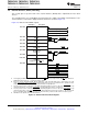
3.6 Interrupts
Figure 3-6 shows how the various interrupt sources are multiplexed within the F281x and C281x devices.
A. Out of a possible 96 interrupts, 45 are currently used by peripherals.
Figure 3-6. Interrupt Sources
Eight PIE block interrupts are grouped into one CPU interrupt. In total, 12 CPU interrupt groups, with
8 interrupts per group equals 96 possible interrupts. On the F281x and C281x, 45 of these are used by
peripherals as shown in Table 3-12.
The TRAP #VectorNumber instruction transfers program control to the interrupt service routine
corresponding to the vector specified. TRAP #0 attempts to transfer program control to the address
pointed to by the reset vector. The PIE vector table does not, however, include a reset vector. Therefore,
TRAP #0 should not be used when the PIE is enabled. Doing so will result in undefined behavior.
When the PIE is enabled, TRAP #1 through TRAP #12 will transfer program control to the interrupt service
routine corresponding to the first vector within the PIE group. For example: TRAP #1 fetches the vector
from INT1.1, TRAP #2 fetches the vector from INT2.1 and so forth.
44 Functional Overview Copyright © 2001–2012, Texas Instruments Incorporated
Submit Documentation Feedback
Product Folder Link(s): TMS320F2810 TMS320F2811 TMS320F2812 TMS320C2810 TMS320C2811 TMS320C2812