
Datasheet


TMS320F2810, TMS320F2811, TMS320F2812
TMS320C2810, TMS320C2811, TMS320C2812
SPRS174T –APRIL 2001–REVISED MAY 2012
www.ti.com
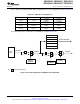
6.21 Serial Peripheral Interface (SPI) Slave Mode Timing
Table 6-28 lists the slave mode timing (clock phase = 0) and Table 6-29 lists the timing (clock phase = 1).
Figure 6-28 and Figure 6-29 show the timing waveforms.
Table 6-28. SPI Slave Mode External Timing (Clock Phase = 0)
(1)(2)
NO. MIN MAX UNIT
12 t
c(SPC)S
Cycle time, SPICLK 4t
c(LCO)
ns
13
(3)
t
w(SPCH)S
Pulse duration, SPICLK high (clock polarity = 0) 0.5t
c(SPC)S
– 10 0.5t
c(SPC)S
ns
t
w(SPCL)S
Pulse duration, SPICLK low (clock polarity = 1) 0.5t
c(SPC)S
– 10 0.5t
c(SPC)S
14
(3)
t
w(SPCL)S
Pulse duration, SPICLK low (clock polarity = 0) 0.5t
c(SPC)S
– 10 0.5t
c(SPC)S
ns
t
w(SPCH)S
Pulse duration, SPICLK high (clock polarity = 1) 0.5t
c(SPC)S
– 10 0.5t
c(SPC)S
15
(3)
t
d(SPCH-SOMI)S
Delay time, SPICLK high to SPISOMI valid (clock polarity = 0) 0.375t
c(SPC)S
– 10 ns
t
d(SPCL-SOMI)S
Delay time, SPICLK low to SPISOMI valid (clock polarity = 1) 0.375t
c(SPC)S
– 10
16
(3)
t
v(SPCL-SOMI)S
Valid time, SPISOMI data valid after SPICLK low (clock polarity = 0) 0.75t
c(SPC)S
ns
t
v(SPCH-SOMI)S
Valid time, SPISOMI data valid after SPICLK high (clock polarity = 1) 0.75t
c(SPC)S
19
(3)
t
su(SIMO-SPCL)S
Setup time, SPISIMO before SPICLK low (clock polarity = 0) 0 ns
t
su(SIMO-SPCH)S
Setup time, SPISIMO before SPICLK high (clock polarity = 1) 0
20
(3)
t
v(SPCL-SIMO)S
Valid time, SPISIMO data valid after SPICLK low (clock polarity = 0) 0.5t
c(SPC)S
ns
t
v(SPCH-SIMO)S
Valid time, SPISIMO data valid after SPICLK high (clock polarity = 1) 0.5t
c(SPC)S
(1) The MASTER/SLAVE bit (SPICTL.2) is cleared and the CLOCK PHASE bit (SPICTL.3) is cleared.
(2) t
c(SPC)
= SPI clock cycle time = LSPCLK/4 or LSPCLK/(SPIBRR + 1)
t
c(LCO)
= LSPCLK cycle time
(3) The active edge of the SPICLK signal referenced is controlled by the CLOCK POLARITY bit (SPICCR.6).
NOTE: Internal clock prescalers must be adjusted such that the SPI clock speed is limited to the following SPI clock rate:
• Master mode transmit: 20 MHz MAX. Master mode receive: 12.5 MHz MAX.
• Slave mode transmit: 12.5 MHz MAX. Slave mode receive: 12.5 MHz MAX.
122 Electrical Specifications Copyright © 2001–2012, Texas Instruments Incorporated
Submit Documentation Feedback
Product Folder Link(s): TMS320F2810 TMS320F2811 TMS320F2812 TMS320C2810 TMS320C2811 TMS320C2812