
Datasheet


TMS320F2810, TMS320F2811, TMS320F2812
TMS320C2810, TMS320C2811, TMS320C2812
SPRS174T –APRIL 2001–REVISED MAY 2012
www.ti.com
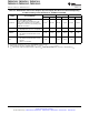
Table 6-2. TMS320C281x Current Consumption by Power-Supply Pins Over Recommended Operating
Conditions During Low-Power Modes at 150-MHz SYSCLKOUT
I
DD
I
DDIO
(1)
I
DDA
(2)
MODE TEST CONDITIONS
TYP MAX
(3)
TYP MAX
(3)
TYP MAX
(3)
All peripheral clocks are enabled. All PWM
pins are toggled at 100 kHz.
Data is continuously transmitted out of the
Operational 210 mA
(4)
260 mA 20 mA 30 mA 40 mA 50 mA
SCIA, SCIB, and CAN ports. The hardware
multiplier is exercised. Code is running out of
ROM with 5 wait-states.
• XCLKOUT is turned off
IDLE 140 mA 165 mA 20 mA 30 mA 5 µA 10 µA
• All peripheral clocks are on, except ADC
• Peripheral clocks are turned off
STANDBY 5 mA 10 mA 5 µA 20 µA 5 µA 10 µA
• Pins without an internal PU/PD are tied
high/low
• Peripheral clocks are turned off
• Pins without an internal PU/PD are tied
HALT 70 µA 5 µA 10 µA 1 µA
high/low
• Input clock is disabled
(1) I
DDIO
current is dependent on the electrical loading on the I/O pins.
(2) I
DDA
includes current into V
DDA1
, V
DDA2
, AVDDREFBG, and V
DDAIO
pins.
(3) MAX numbers are at 125°C, and MAX voltage (V
DD
= 1.89 V; V
DDIO
, V
DD3VFL
, V
DDA
= 3.47 V).
(4) I
DD
represents the total current drawn from the 1.8-V rail (V
DD
). It includes a small amount of current (<1 mA) drawn by V
DD1
.
94 Electrical Specifications Copyright © 2001–2012, Texas Instruments Incorporated
Submit Documentation Feedback
Product Folder Link(s): TMS320F2810 TMS320F2811 TMS320F2812 TMS320C2810 TMS320C2811 TMS320C2812