
Datasheet


Analog Input on
Channel Ax or Bx
ADC Clock
Sample and Hold
SH Pulse
SMODE Bit
t
dschx_n
t
dschx_n+1
Sample n
Sample n+1
Sample n+2
t
SH
ADC Event Trigger from EV
or Other Sources
t
d(SH)
TMS320F2810, TMS320F2811, TMS320F2812
TMS320C2810, TMS320C2811, TMS320C2812
www.ti.com
SPRS174T –APRIL 2001–REVISED MAY 2012
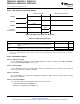
6.30.6 Sequential Sampling Mode (Single-Channel) (SMODE = 0)
In sequential sampling mode, the ADC can continuously convert input signals on any of the channels (Ax
to Bx). The ADC can start conversions on event triggers from the Event Managers (EVA/EVB), software
trigger, or from an external ADCSOC signal. If the SMODE bit is 0, the ADC will do conversions on the
selected channel on every Sample/Hold pulse. The conversion time and latency of the Result register
update are explained below. The ADC interrupt flags are set a few SYSCLKOUT cycles after the Result
register update. The selected channels will be sampled at every falling edge of the Sample/Hold pulse.
The Sample/Hold pulse width can be programmed to be 1 ADC clock wide (minimum) or 16 ADC clocks
wide (maximum).
Figure 6-41. Sequential Sampling Mode (Single-Channel) Timing
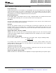
Table 6-48. Sequential Sampling Mode Timing
AT 25-MHz
SAMPLE n SAMPLE n + 1 ADC CLOCK, REMARKS
t
c(ADCCLK)
= 40 ns
Delay time from event
t
d(SH)
2.5t
c(ADCCLK)
trigger to sampling
Sample/
Acqps value = 0–15
t
SH
Hold width/ (1 + Acqps) * t
c(ADCCLK)
40 ns with Acqps = 0
ADCTRL1[8:11]
Acquisition width
Delay time for first
t
d(schx_n)
result to appear in the 4t
c(ADCCLK)
160 ns
Result register
Delay time for
successive results to
t
d(schx_n+1)
(2 + Acqps) * t
c(ADCCLK)
80 ns
appear in the Result
register
Copyright © 2001–2012, Texas Instruments Incorporated Electrical Specifications 147
Submit Documentation Feedback
Product Folder Link(s): TMS320F2810 TMS320F2811 TMS320F2812 TMS320C2810 TMS320C2811 TMS320C2812