
Datasheet


TMS320F2810, TMS320F2811, TMS320F2812
TMS320C2810, TMS320C2811, TMS320C2812
SPRS174T –APRIL 2001–REVISED MAY 2012
www.ti.com
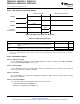
6.30.2 ADC Electrical Characteristics Over Recommended Operating Conditions
Table 6-44. DC Specifications
(1)
PARAMETER MIN TYP MAX UNIT
Resolution 12 Bits
1 kHz
ADC clock
(2)
25 MHz
ACCURACY
INL (Integral nonlinearity)
(3)
1–18.75 MHz ADC clock ±1.5 LSB
DNL (Differential nonlinearity)
(3)
1–18.75 MHz ADC clock ±1 LSB
Offset error
(4)
–80 80 LSB
F281x –200 200
Overall gain error with internal reference
(5)
LSB
C281x –80 80
Overall gain error with external reference
(6)
If ADCREFP – ADCREFM = 1 V ± 0.1% –50 50 LSB
Channel-to-channel offset variation ±8 LSB
Channel-to-channel Gain variation ±8 LSB
ANALOG INPUT
Analog input voltage (ADCINx to ADCLO)
(7)
0 3 V
ADCLO –5 0 5 mV
Input capacitance 10 pF
Input leakage current 3 ±5 µA
INTERNAL VOLTAGE REFERENCE
(5)
Accuracy, ADCV
REFP
1.9 2 2.1 V
Accuracy, ADCV
REFM
0.95 1 1.05 V
Voltage difference, ADCREFP – ADCREFM 1 V
Temperature coefficient 50 PPM/°C
Reference noise 100 µV
EXTERNAL VOLTAGE REFERENCE
(6)
Accuracy, ADCV
REFP
1.9 2 2.1 V
Accuracy, ADCV
REFM
0.95 1 1.05 V
Input voltage difference, ADCREFP – ADCREFM 0.99 1 1.01 V
(1) Tested at 12.5-MHz ADCCLK.
(2) If SYSCLKOUT ≤ 25 MHz, ADC clock ≤ SYSCLKOUT/2.
(3) The INL degrades for frequencies beyond 18.75 MHz–25 MHz. Applications that require these sampling rates should use a 20K resistor
as bias resistor on the ADCRESEXT pin. This improves overall linearity and typical current drawn by the ADC will be a few mA more
than 24.9-kΩ bias. The ADC module in C281x devices can operate at 24.9k bias on ADCRESEXT pin for the full range 1–25 MHz.
(4) 1 LSB has the weighted value of 3.0/4096 = 0.732 mV.
(5) A single internal band gap reference (±5% accuracy) sources both ADCREFP and ADCREFM signals, and hence, these voltages track
together. The ADC converter uses the difference between these two as its reference. The total gain error will be the combination of the
gain error shown here and the voltage reference accuracy (ADCREFP – ADCREFM). A software-based calibration procedure is
recommended for better accuracy. See the F2810, F2811, and F2812 ADC Calibration Application Report (literature number SPRA989)
and Section 5.2, Documentation Support, for relevant documents.
(6) In this mode, the accuracy of external reference is critical for overall gain. The voltage difference (ADCREFP – ADCREFM) will
determine the overall accuracy.
(7) Voltages above V
DDA
+ 0.3 V or below V
SS
– 0.3 V applied to an analog input pin may temporarily affect the conversion of another pin.
To avoid this, the analog inputs should be kept within these limits.
144 Electrical Specifications Copyright © 2001–2012, Texas Instruments Incorporated
Submit Documentation Feedback
Product Folder Link(s): TMS320F2810 TMS320F2811 TMS320F2812 TMS320C2810 TMS320C2811 TMS320C2812