
Datasheet


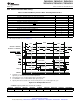


Lead
Active
Trail
t
d(XCOH-XZCSL)
t
d(XCOH-XA)
t
d(XCOHL-XWEL)
t
d(XCOHL-XWEH)
t
d(XCOHL-XZCSH)
t
en(XD)XWEL
t
h(XD)XWEH
t
dis(XD)XRNW
XCLKOUT = XTIMCLK
XCLKOUT = 1/2 XTIMCLK
XZCS0AND1 XZCS2
XZCS6AND7
, ,
XA[0:18]
XRD
XWE
XR/W
XD[0:15]
t
d(XCOH-XRNWL)
t
d(XCOHL-XRNWH)
DOUT
XREADY
t
d(XWEL-XD)
TMS320F2810, TMS320F2811, TMS320F2812
TMS320C2810, TMS320C2811, TMS320C2812
www.ti.com
SPRS174T –APRIL 2001–REVISED MAY 2012
6.25 External Interface Write Timing
Table 6-34. External Memory Interface Write Switching Characteristics
PARAMETER MIN MAX UNIT
t
d(XCOH-XZCSL)
Delay time, XCLKOUT high to zone chip-select active-low 1 ns
t
d(XCOHL-XZCSH)
Delay time, XCLKOUT high or low to zone chip-select inactive-high –2 3 ns
t
d(XCOH-XA)
Delay time, XCLKOUT high to address valid 2 ns
t
d(XCOHL-XWEL)
Delay time, XCLKOUT high/low to XWE low 2 ns
t
d(XCOHL-XWEH)
Delay time, XCLKOUT high/low to XWE high 2 ns
t
d(XCOH-XRNWL)
Delay time, XCLKOUT high to XR/W low 1 ns
t
d(XCOHL-XRNWH)
Delay time, XCLKOUT high/low to XR/W high –2 1 ns
t
en(XD)XWEL
Enable time, data bus driven from XWE low 0 ns
t
d(XWEL-XD)
Delay time, data valid after XWE active-low 4 ns
t
h(XA)XZCSH
Hold time, address valid after zone chip-select inactive-high
(1)
ns
t
h(XD)XWE
Hold time, write data valid after XWE inactive-high TW – 2
(2)
ns
t
dis(XD)XRNW
Maximum time for DSP to release the data bus after XR/W inactive-high 4 ns
(1) During inactive cycles, the XINTF address bus will always hold the last address put out on the bus. This includes alignment cycles.
(2) TW = Trail period, write access. See Table 6-30.
A. All XINTF accesses (lead period) begin on the rising edge of XCLKOUT. When necessary, the device will insert an
alignment cycle before an access to meet this requirement.
B. During alignment cycles, all signals will transition to their inactive state.
C. For USEREADY = 0, the external XREADY input signal is ignored.
D. XA[0:18] will hold the last address put on the bus during inactive cycles, including alignment cycles.
Figure 6-32. Example Write Access
XTIMING register parameters used for this example:
XRDLEAD XRDACTIVE XRDTRAIL USEREADY X2TIMING XWRLEAD XWRACTIVE XWRTRAIL READYMODE
N/A
(1)
N/A
(1)
N/A
(1)
0 0 ≥ 1 ≥ 0 ≥ 0 N/A
(1)
(1) N/A = “Don’t care” for this example
Copyright © 2001–2012, Texas Instruments Incorporated Electrical Specifications 133
Submit Documentation Feedback
Product Folder Link(s): TMS320F2810 TMS320F2811 TMS320F2812 TMS320C2810 TMS320C2811 TMS320C2812