
Datasheet


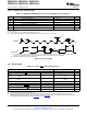


XCLKOUT
(A)(B)
XCLKIN
(A)
C10
C3
C4
C9
C5
C8
C1
C6
TMS320F2810, TMS320F2811, TMS320F2812
TMS320C2810, TMS320C2811, TMS320C2812
SPRS174T –APRIL 2001–REVISED MAY 2012
www.ti.com
6.14.2 Output Clock Characteristics
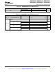
Table 6-10. XCLKOUT Switching Characteristics (PLL Bypassed or Enabled)
(1)(2)
NO. PARAMETER MIN TYP MAX UNIT
C1 t
c(XCO)
Cycle time, XCLKOUT 6.67
(3)
ns
C3 t
f(XCO)
Fall time, XCLKOUT 2 ns
C4 t
r(XCO)
Rise time, XCLKOUT 2 ns
C5 t
w(XCOL)
Pulse duration, XCLKOUT low H – 2 H + 2 ns
C6 t
w(XCOH)
Pulse duration, XCLKOUT high H – 2 H + 2 ns
C7 t
p
PLL lock time
(4)
131072t
c(CI)
ns
(1) A load of 40 pF is assumed for these parameters.
(2) H = 0.5t
c(XCO)
(3) The PLL must be used for maximum frequency operation.
(4) This parameter has changed from 4096 XCLKIN cycles in the earlier revisions of the silicon.
A. The relationship of XCLKIN to XCLKOUT depends on the divide factor chosen. The waveform relationship shown in
Figure 6-10 is intended to illustrate the timing parameters only and may differ based on configuration.
B. XCLKOUT configured to reflect SYSCLKOUT.
Figure 6-10. Clock Timing
6.15 Reset Timing
Table 6-11. Reset (XRS) Timing Requirements
(1)
MIN NOM MAX UNIT
t
w(RSL1)
Pulse duration, stable XCLKIN to XRS high 8t
c(CI)
cycles
t
w(RSL2)
Pulse duration, XRS low Warm reset 8t
c(CI)
cycles
Pulse duration, reset pulse generated by
t
w(WDRS)
512t
c(CI)
cycles
watchdog
Delay time, address/data valid after XRS
t
d(EX)
32t
c(CI)
cycles
high
t
OSCST
(2)
Oscillator start-up time 1 10 ms
t
su(XPLLDIS)
Setup time for XPLLDIS pin 16t
c(CI)
cycles
t
h(XPLLDIS)
Hold time for XPLLDIS pin 16t
c(CI)
cycles
t
h(XMP/MC)
Hold time for XMP/MC pin 16t
c(CI)
cycles
t
h(boot-mode)
Hold time for boot-mode pins 2520t
c(CI)
(3)
cycles
(1) If external oscillator/clock source are used, reset time has to be low at least for 1 ms after V
DD
reaches 1.5 V.
(2) Dependent on crystal/resonator and board design.
(3) The boot ROM reads the password locations. Therefore, this timing requirement includes the wakeup time for flash. See the
TMS320x281x DSP Boot ROM Reference Guide (literature number SPRU095) and the TMS320x281x DSP System Control and
Interrupts Reference Guide (literature number SPRU078) for further information.
104 Electrical Specifications Copyright © 2001–2012, Texas Instruments Incorporated
Submit Documentation Feedback
Product Folder Link(s): TMS320F2810 TMS320F2811 TMS320F2812 TMS320C2810 TMS320C2811 TMS320C2812