
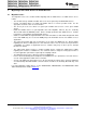
Datasheet


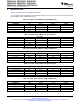


+
ƪ
ǒ
t
a(rp)
t
c(SCO)
Ǔ* 1
ƫ(round up to the next highest integer) or 0, whichever is larger
+
ƪ
ǒ
t
a(rr)
t
c(SCO)
Ǔ* 1
ƫ
(round up to the next highest integer) or 1, whichever is larger
ROM Page Wait-State
ROM Random Wait-State
TMS320F2809, TMS320F2808, TMS320F2806
TMS320F2802, TMS320F2801, TMS320C2802
TMS320C2801, TMS320F28016, TMS320F28015
www.ti.com
SPRS230N –OCTOBER 2003–REVISED MAY 2012
6.13 ROM Timing (C280x only)
Table 6-48. ROM/OTP Access Timing
PARAMETER MIN TYP MAX UNIT
t
a(rp)
Paged ROM access time 19 ns
t
a(rr)
Random ROM access time 19 ns
t
a(ROM)
ROM (OTP area) access time
(1)
60 ns
(1) In C280x devices, a 1K X 16 ROM block replaces the OTP block found in Flash devices.
Equations to compute the page wait-state and random wait-state in Table 6-49 are as follows:
Table 6-49. ROM/ROM (OTP area) Minimum Required
Wait-States at Different Frequencies
SYSCLKOUT SYSCLKOUT PAGE WAIT- RANDOM WAIT-
(MHz) (ns) STATE STATE
(1)
100 10 1 1
75 13.33 1 1
50 20 0 1
30 33.33 0 1
25 40 0 1
15 66.67 0 1
4 250 0 1
(1) Random wait-state must be greater than or equal to 1.
Copyright © 2003–2012, Texas Instruments Incorporated Electrical Specifications 133
Submit Documentation Feedback
Product Folder Link(s): TMS320F2809 TMS320F2808 TMS320F2806 TMS320F2802 TMS320F2801 TMS320C2802
TMS320C2801 TMS320F28016 TMS320F28015