
Datasheet


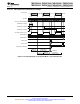


ADCPWDN/
ADCBGPWD/
ADCREFPWD/
ADCENABLE
Request for ADC
Conversion
t
d(PWD)
TMS320F28069, TMS320F28068, TMS320F28067, TMS320F28066
TMS320F28065, TMS320F28064, TMS320F28063, TMS320F28062
www.ti.com
SPRS698D –NOVEMBER 2010–REVISED DECEMBER 2012
Table 5-22. ADC Power Modes
ADC OPERATING MODE CONDITIONS I
DDA
UNITS
Mode A – Operating Mode ADC Clock Enabled 16 mA
Bandgap On (ADCBGPWD = 1)
Reference On (ADCREFPWD = 1)
ADC Powered Up (ADCPWDN = 1)
Mode B – Quick Wake Mode ADC Clock Enabled 4 mA
Bandgap On (ADCBGPWD = 1)
Reference On (ADCREFPWD = 1)
ADC Powered Up (ADCPWDN = 0)
Mode C – Comparator-Only Mode ADC Clock Enabled 1.5 mA
Bandgap On (ADCBGPWD = 1)
Reference On (ADCREFPWD = 0)
ADC Powered Up (ADCPWDN = 0)
Mode D – Off Mode ADC Clock Enabled 0.075 mA
Bandgap On (ADCBGPWD = 0)
Reference On (ADCREFPWD = 0)
ADC Powered Up (ADCPWDN = 0)
5.10.1.3.1 Internal Temperature Sensor
Table 5-23. Temperature Sensor Coefficient
PARAMETER
(1)
MIN TYP MAX UNIT
T
SLOPE
Degrees C of temperature movement per measured ADC LSB change of the 0.18
(2)(3)
°C/LSB
temperature sensor
T
OFFSET
ADC output at 0°C of the temperature sensor 1750 LSB
(1) The temperature sensor slope and offset are given in terms of ADC LSBs using the internal reference of the ADC. Values must be
adjusted accordingly in external reference mode to the external reference voltage.
(2) ADC temperature coeffieicient is accounted for in this specification
(3) Output of the temperature sensor (in terms of LSBs) is sign-consistent with the direction of the temperature movement. Increasing
temperatures will give increasing ADC values relative to an initial value; decreasing temperatures will give decreasing ADC values
relative to an initial value.
5.10.1.3.2 ADC Power-Up Control Bit Timing
Table 5-24. ADC Power-Up Delays
PARAMETER
(1)
MIN MAX UNIT
t
d(PWD)
Delay time for the ADC to be stable after power up 1 ms
(1) Timings maintain compatibility to the ADC module. The 2806x ADC supports driving all 3 bits at the same time t
d(PWD)
ms before first
conversion.
Figure 5-17. ADC Conversion Timing
Copyright © 2010–2012, Texas Instruments Incorporated Peripheral and Electrical Specifications 87
Submit Documentation Feedback
Product Folder Links: TMS320F28069 TMS320F28068 TMS320F28067 TMS320F28066 TMS320F28065
TMS320F28064 TMS320F28063 TMS320F28062