
Datasheet


TMS320F28030, TMS320F28031, TMS320F28032
TMS320F28033, TMS320F28034, TMS320F28035
SPRS584J –APRIL 2009–REVISED OCTOBER 2013
www.ti.com
2.2 Signal Descriptions
Table 2-2 describes the signals. With the exception of the JTAG pins, the GPIO function is the default at
reset, unless otherwise mentioned. The peripheral signals that are listed under them are alternate
functions. Some peripheral functions may not be available in all devices. See Table 2-1 for details. Inputs
are not 5-V tolerant. All GPIO pins are I/O/Z and have an internal pullup, which can be selectively
enabled/disabled on a per-pin basis. This feature only applies to the GPIO pins. The pullups on the PWM
pins are not enabled at reset. The pullups on other GPIO pins are enabled upon reset. The AIO pins do
not have an internal pullup.
NOTE: When the on-chip VREG is used, the GPIO19, GPIO34, GPIO35, GPIO36, GPIO37, and GPIO38
pins could glitch during power up. If this is unacceptable in an application, 1.8 V could be supplied
externally. There is no power-sequencing requirement when using an external 1.8-V supply. However, if
the 3.3-V transistors in the level-shifting output buffers of the I/O pins are powered prior to the 1.9-V
transistors, it is possible for the output buffers to turn on, causing a glitch to occur on the pin during power
up. To avoid this behavior, power the V
DD
pins prior to or simultaneously with the V
DDIO
pins, ensuring that
the V
DD
pins have reached 0.7 V before the V
DDIO
pins reach 0.7 V.
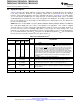
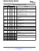
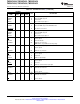
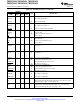
Table 2-2. Terminal Functions
(1)
TERMINAL
I/O/Z DESCRIPTION
PN PAG RSH
NAME
PIN # PIN # PIN #
JTAG
JTAG test reset with internal pulldown. TRST, when driven high, gives the scan
system control of the operations of the device. If this signal is not connected or
driven low, the device operates in its functional mode, and the test reset signals
are ignored. NOTE: TRST is an active high test pin and must be maintained low
at all times during normal device operation. An external pull-down resistor is
TRST 10 8 6 I
required on this pin. The value of this resistor should be based on drive strength
of the debugger pods applicable to the design. A 2.2-kΩ resistor generally offers
adequate protection. Since this is application-specific, it is recommended that
each target board be validated for proper operation of the debugger and the
application. (↓)
TCK See GPIO38 I See GPIO38. JTAG test clock with internal pullup. (↑)
See GPIO36. JTAG test-mode select (TMS) with internal pullup. This serial
TMS See GPIO36 I
control input is clocked into the TAP controller on the rising edge of TCK.. (↑)
See GPIO35. JTAG test data input (TDI) with internal pullup. TDI is clocked into
TDI See GPIO35 I
the selected register (instruction or data) on a rising edge of TCK. (↑)
See GPIO37. JTAG scan out, test data output (TDO). The contents of the
TDO See GPIO37 O/Z selected register (instruction or data) are shifted out of TDO on the falling edge of
TCK. (8 mA drive)
FLASH
TEST2 38 30 27 I/O Test Pin. Reserved for TI. Must be left unconnected.
(1) I = Input, O = Output, Z = High Impedance, OD = Open Drain, ↑ = Pullup, ↓ = Pulldown
14 Introduction Copyright © 2009–2013, Texas Instruments Incorporated
Submit Documentation Feedback
Product Folder Links: TMS320F28030 TMS320F28031 TMS320F28032 TMS320F28033 TMS320F28034
TMS320F28035