
Datasheet


To COMPy A or B input
To ADC Channel X
1
0
AIOx Pin
AIOxIN
AIOxINE
SYNC
SYSCLK
Logic implemented in GPIO MUX block
AIODAT Reg
(Read)
AIODAT Reg
(Latch)
AIOSET,
AIOCLEAR,
AIOTOGGLE
Regs
AIOMUX 1 Reg
1
0
AIOxDIR
(1 = Input,
0 = Output)
(0 = Input, 1 = Output)
AIODIR Reg
(Latch)
0
TMS320F28030, TMS320F28031, TMS320F28032
TMS320F28033, TMS320F28034, TMS320F28035
www.ti.com
SPRS584J –APRIL 2009–REVISED OCTOBER 2013
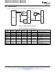
4.2.2 ADC MUX
Figure 4-4. AIOx Pin Multiplexing
The ADC channel and Comparator functions are always available. The digital I/O function is available only
when the respective bit in the AIOMUX1 register is 0. In this mode, reading the AIODAT register reflects
the actual pin state.
The digital I/O function is disabled when the respective bit in the AIOMUX1 register is 1. In this mode,
reading the AIODAT register reflects the output latch of the AIODAT register and the input digital I/O buffer
is disabled to prevent analog signals from generating noise.
On reset, the digital function is disabled. If the pin is used as an analog input, users should keep the AIO
function disabled for that pin.
Copyright © 2009–2013, Texas Instruments Incorporated Peripherals 63
Submit Documentation Feedback
Product Folder Links: TMS320F28030 TMS320F28031 TMS320F28032 TMS320F28033 TMS320F28034
TMS320F28035