
Datasheet


TMS320F28030, TMS320F28031, TMS320F28032
TMS320F28033, TMS320F28034, TMS320F28035
SPRS584J –APRIL 2009–REVISED OCTOBER 2013
www.ti.com
NOTE
• When the code-security passwords are programmed, all addresses between 0x3F 7F80
and 0x3F 7FF5 cannot be used as program code or data. These locations must be
programmed to 0x0000.
• If the code security feature is not used, addresses 0x3F 7F80 through 0x3F 7FEF may
be used for code or data. Addresses 0x3F 7FF0 – 0x3F 7FF5 are reserved for data and
should not contain program code.
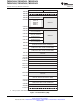
Table 3-4 shows how to handle these memory locations.
Table 3-4. Impact of Using the Code Security Module
FLASH
ADDRESS
CODE SECURITY ENABLED CODE SECURITY DISABLED
0x3F 7F80 – 0x3F 7FEF Application code and data
Fill with 0x0000
0x3F 7FF0 – 0x3F 7FF5 Reserved for data only
Peripheral Frame 1, Peripheral Frame 2, and Peripheral Frame 3 are grouped together to enable these
blocks to be write/read peripheral block protected. The protected mode makes sure that all accesses to
these blocks happen as written. Because of the pipeline, a write immediately followed by a read to
different memory locations, will appear in reverse order on the memory bus of the CPU. This can cause
problems in certain peripheral applications where the user expected the write to occur first (as written).
The CPU supports a block protection mode where a region of memory can be protected so that operations
occur as written (the penalty is extra cycles are added to align the operations). This mode is
programmable and by default, it protects the selected zones.
The wait-states for the various spaces in the memory map area are listed in Table 3-5.
Table 3-5. Wait-States
AREA WAIT-STATES (CPU) COMMENTS
M0 and M1 SARAMs 0-wait Fixed
Peripheral Frame 0 0-wait
Peripheral Frame 1 0-wait (writes) Cycles can be extended by peripheral generated ready.
2-wait (reads) Back-to-back write operations to Peripheral Frame 1 registers will incur
a 1-cycle stall (1-cycle delay).
Peripheral Frame 2 0-wait (writes) Fixed. Cycles cannot be extended by the peripheral.
2-wait (reads)
Peripheral Frame 3 0-wait (writes) Assumes no conflict between CPU and CLA.
2-wait (reads) Cycles can be extended by peripheral-generated ready.
L0 SARAM 0-wait data and program Assumes no CPU conflicts
L1 SARAM 0-wait data and program Assumes no CPU conflicts
L2 SARAM 0-wait data and program Assumes no CPU conflicts
L3 SARAM 0-wait data and program Assumes no CPU conflicts
OTP Programmable Programmed via the Flash registers.
1-wait minimum 1-wait is minimum number of wait states allowed.
FLASH Programmable Programmed via the Flash registers.
0-wait Paged min
1-wait Random min
Random ≥ Paged
FLASH Password 16-wait fixed Wait states of password locations are fixed.
Boot-ROM 0-wait
28 Functional Overview Copyright © 2009–2013, Texas Instruments Incorporated
Submit Documentation Feedback
Product Folder Links: TMS320F28030 TMS320F28031 TMS320F28032 TMS320F28033 TMS320F28034
TMS320F28035