
Datasheet


TMS320F28030, TMS320F28031, TMS320F28032
TMS320F28033, TMS320F28034, TMS320F28035
SPRS584J –APRIL 2009–REVISED OCTOBER 2013
www.ti.com
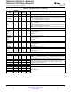
Table 2-2. Terminal Functions
(1)
(continued)
TERMINAL
I/O/Z DESCRIPTION
PN PAG RSH
NAME
PIN # PIN # PIN #
ADCINA1 17 14 12 I ADC Group A, Channel 1 input
ADC Group A, Channel 0 input.
NOTE: V
REFHI
and ADCINA0 share the same pin on the 64-pin PAG device and
ADCINA0 18 15 13 I their use is mutually exclusive to one another.
NOTE: V
REFHI
and ADCINA0 share the same pin on the 56-pin RSH device and
their use is mutually exclusive to one another.
ADC External Reference – only used when in ADC external reference mode. See
Section 4.2.1, ADC.
NOTE: V
REFHI
and ADCINA0 share the same pin on the 64-pin PAG device and
V
REFHI
19 15 13 I
their use is mutually exclusive to one another.
NOTE: V
REFHI
and ADCINA0 share the same pin on the 56-pin RSH device and
their use is mutually exclusive to one another.
ADCINB7 30 24 21 I ADC Group B, Channel 7 input
ADCINB6 29 23 20 I ADC Group B, Channel 6 input
COMP3B I Comparator Input 3B
AIO14 I/O Digital AIO 14
ADCINB5 28 – – I ADC Group B, Channel 5 input
ADCINB4 27 22 19 I ADC Group B, Channel 4 input
COMP2B I Comparator Input 2B
AIO12 I/O Digital AIO12
ADCINB3 26 21 18 I ADC Group B, Channel 3 input
ADCINB2 25 20 17 I ADC Group B, Channel 2 input
COMP1B I Comparator Input 1B
AIO10 I/O Digital AIO 10
ADCINB1 24 19 16 I ADC Group B, Channel 1 input
ADCINB0 23 18 – I ADC Group B, Channel 0 input
NOTE: V
REFLO
is always connected to V
SSA
on the 64-pin PAG device and on the
V
REFLO
22 17 15 I
56-pin RSH device.
CPU AND I/O POWER
V
DDA
20 16 14 Analog Power Pin. Tie with a 2.2-μF capacitor (typical) close to the pin.
Analog Ground Pin.
V
SSA
21 17 15 NOTE: V
REFLO
is always connected to V
SSA
on the 64-pin PAG device and on the
56-pin RSH device.
V
DD
7 5 3 CPU and Logic Digital Power Pins – no supply source needed when using
internal VREG. Tie with 1.2 µF (minimum) ceramic capacitor (10% tolerance) to
V
DD
54 43 38
ground when using internal VREG. Higher value capacitors may be used, but
V
DD
72 59 52
could impact supply-rail ramp-up time.
V
DDIO
36 29 26
Digital I/O and Flash Power Pin – Single Supply source when VREG is enabled
V
DDIO
70 57 50
V
SS
8 6 4
V
SS
35 28 25
Digital Ground Pins
V
SS
53 42 37
V
SS
71 58 51
16 Introduction Copyright © 2009–2013, Texas Instruments Incorporated
Submit Documentation Feedback
Product Folder Links: TMS320F28030 TMS320F28031 TMS320F28032 TMS320F28033 TMS320F28034
TMS320F28035