
Datasheet


TMS320F28030, TMS320F28031, TMS320F28032
TMS320F28033, TMS320F28034, TMS320F28035
www.ti.com
SPRS584J –APRIL 2009–REVISED OCTOBER 2013
6.11.13 On-Chip Analog-to-Digital Converter
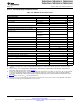
Table 6-37. ADC Electrical Characteristics
PARAMETER MIN TYP MAX UNIT
DC SPECIFICATIONS
Resolution 12 Bits
ADC clock 60-MHz device 0.001 60 MHz
Sample Window 28035/34/33/32 7 64 ADC
Clocks
28031/30 24 64
ACCURACY
INL (Integral nonlinearity) at ADC Clock ≤ 30 MHz
(1)
–4 4 LSB
DNL (Differential nonlinearity) at ADC Clock ≤ 30 MHz, –1 1 LSB
no missing codes
Offset error
(2)
Executing a single self- –20 0 20 LSB
recalibration
(3)
Executing periodic self- –4 0 4
recalibration
(4)
Overall gain error with internal reference –60 60 LSB
Overall gain error with external reference –40 40 LSB
Channel-to-channel offset variation –4 4 LSB
Channel-to-channel gain variation –4 4 LSB
ADC temperature coefficient with internal reference –50 ppm/°C
ADC temperature coefficient with external reference –20 ppm/°C
V
REFLO
–100 µA
V
REFHI
100 µA
ANALOG INPUT
Analog input voltage with internal reference 0 3.3 V
Analog input voltage with external reference V
REFLO
V
REFHI
V
V
REFLO
input voltage
(5)
V
SSA
0.66 V
V
REFHI
input voltage
(6)
2.64 V
DDA
V
with V
REFLO
= V
SSA
1.98 V
DDA
Input capacitance 5 pF
Input leakage current ±2 μA
(1) INL will degrade when the ADC input voltage goes above V
DDA
.
(2) 1 LSB has the weighted value of full-scale range (FSR)/4096. FSR is 3.3 V with internal reference and V
REFHI
- V
REFLO
for external
reference.
(3) For more details, see the TMS320F28030, TMS320F28031, TMS320F28032, TMS320F28033, TMS320F28034, TMS320F28035
Piccolo MCU Silicon Errata (literature number SPRZ295).
(4) Periodic self-recalibration will remove system-level and temperature dependencies on the ADC zero offset error. This can be performed
as needed in the application without sacrificing an ADC channel by using the procedure listed in the "ADC Zero Offset Calibration"
section of the TMS320x2802x, 2803x Piccolo Analog-to-Digital Converter (ADC) and Comparator Reference Guide (literature number
SPRUGE5).
(5) V
REFLO
is always connected to V
SSA
on the 64-pin PAG device.
(6) V
REFHI
must not exceed V
DDA
when using either internal or external reference modes. Since V
REFHI
is tied to ADCINA0 on the 64-pin
PAG device, the input signal on ADCINA0 must not exceed V
DDA
.
Copyright © 2009–2013, Texas Instruments Incorporated Electrical Specifications 137
Submit Documentation Feedback
Product Folder Links: TMS320F28030 TMS320F28031 TMS320F28032 TMS320F28033 TMS320F28034
TMS320F28035