
Datasheet


DataValid
22
SPISIMO
SPISOMI
SPICLK
(clockpolarity=1)
SPICLK
(clockpolarity=0)
SPISIMOdata
mustbevalid
SPISOMIdataisvalid
21
12
18
17
14
13
SPISTE
(A)
TMS320F28030, TMS320F28031, TMS320F28032
TMS320F28033, TMS320F28034, TMS320F28035
www.ti.com
SPRS584J –APRIL 2009–REVISED OCTOBER 2013
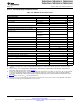
Table 6-35. SPI Slave Mode External Timing (Clock Phase = 1)
(1)(2)(3)(4)
NO. MIN MAX UNIT
12 t
c(SPC)S
Cycle time, SPICLK 8t
c(LCO)
ns
13 t
w(SPCH)S
Pulse duration, SPICLK high (clock polarity = 0) 0.5t
c(SPC)S
– 10 0.5t
c(SPC)S
ns
t
w(SPCL)S
Pulse duration, SPICLK low (clock polarity = 1) 0.5t
c(SPC)S
– 10 0.5t
c(SPC) S
14 t
w(SPCL)S
Pulse duration, SPICLK low (clock polarity = 0) 0.5t
c(SPC)S
– 10 0.5t
c(SPC) S
ns
t
w(SPCH)S
Pulse duration, SPICLK high (clock polarity = 1) 0.5t
c(SPC)S
– 10 0.5t
c(SPC)S
17 t
su(SOMI-SPCH)S
Setup time, SPISOMI before SPICLK high (clock polarity = 0) 0.125t
c(SPC)S
ns
t
su(SOMI-SPCL)S
Setup time, SPISOMI before SPICLK low (clock polarity = 1) 0.125t
c(SPC)S
18 t
v(SPCL-SOMI)S
Valid time, SPISOMI data valid after SPICLK low 0.75t
c(SPC)S
ns
(clock polarity = 1)
t
v(SPCH-SOMI)S
Valid time, SPISOMI data valid after SPICLK high 0.75t
c(SPC) S
(clock polarity = 0)
21 t
su(SIMO-SPCH)S
Setup time, SPISIMO before SPICLK high (clock polarity = 0) 26 ns
t
su(SIMO-SPCL)S
Setup time, SPISIMO before SPICLK low (clock polarity = 1) 26
22 t
v(SPCH-SIMO)S
Valid time, SPISIMO data valid after SPICLK high 0.5t
c(SPC)S
– 10 ns
(clock polarity = 0)
t
v(SPCL-SIMO)S
Valid time, SPISIMO data valid after SPICLK low 0.5t
c(SPC)S
– 10
(clock polarity = 1)
(1) The MASTER / SLAVE bit (SPICTL.2) is cleared and the CLOCK PHASE bit (SPICTL.3) is cleared.
(2) t
c(SPC)
= SPI clock cycle time = LSPCLK/4 or LSPCLK/(SPIBRR + 1)
(3) Internal clock prescalers must be adjusted such that the SPI clock speed is limited to the following SPI clock rate:
Master mode transmit 15-MHz MAX, master mode receive 10-MHz MAX
Slave mode transmit 10-MHz MAX, slave mode receive 10-MHz MAX.
(4) The active edge of the SPICLK signal referenced is controlled by the CLOCK POLARITY bit (SPICCR.6).
A. In the slave mode, the SPISTE signal should be asserted low at least 0.5t
c(SPC)
before the valid SPI clock edge and
remain low for at least 0.5t
c(SPC)
after the receiving edge (SPICLK) of the last data bit.
Figure 6-24. SPI Slave Mode External Timing (Clock Phase = 1)
Copyright © 2009–2013, Texas Instruments Incorporated Electrical Specifications 135
Submit Documentation Feedback
Product Folder Links: TMS320F28030 TMS320F28031 TMS320F28032 TMS320F28033 TMS320F28034
TMS320F28035