
Datasheet


TMS320F28027, TMS320F28026, TMS320F28023, TMS320F28022
TMS320F28021, TMS320F28020, TMS320F280200
SPRS523J –NOVEMBER 2008–REVISED OCTOBER 2013
www.ti.com
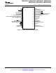
2.2 Signal Descriptions
Table 2-2 describes the signals. With the exception of the JTAG pins, the GPIO function is the default at
reset, unless otherwise mentioned. The peripheral signals that are listed under them are alternate
functions. Some peripheral functions may not be available in all devices. See Table 2-1 for details. Inputs
are not 5-V tolerant. All GPIO pins are I/O/Z and have an internal pullup, which can be selectively
enabled/disabled on a per-pin basis. This feature only applies to the GPIO pins. The pullups on the PWM
pins are not enabled at reset. The pullups on other GPIO pins are enabled upon reset. The AIO pins do
not have an internal pullup.
NOTE: When the on-chip VREG is used, the GPIO19, GPIO34, GPIO35, GPIO36, GPIO37, and GPIO38
pins could glitch during power up. If this is unacceptable in an application, 1.8 V could be supplied
externally. There is no power-sequencing requirement when using an external 1.8-V supply. However, if
the 3.3-V transistors in the level-shifting output buffers of the I/O pins are powered prior to the 1.9-V
transistors, it is possible for the output buffers to turn on, causing a glitch to occur on the pin during power
up. To avoid this behavior, power the V
DD
pins prior to or simultaneously with the V
DDIO
pins, ensuring that
the V
DD
pins have reached 0.7 V before the V
DDIO
pins reach 0.7 V.
Table 2-2. Terminal Functions
(1)
TERMINAL
I/O/Z DESCRIPTION
PT DA
NAME
PIN # PIN #
JTAG
JTAG test reset with internal pulldown. TRST, when driven high, gives the scan
system control of the operations of the device. If this signal is not connected or driven
low, the device operates in its functional mode, and the test reset signals are ignored.
NOTE: TRST is an active high test pin and must be maintained low at all times during
TRST 2 16 I normal device operation. An external pulldown resistor is required on this pin. The
value of this resistor should be based on drive strength of the debugger pods
applicable to the design. A 2.2-kΩ resistor generally offers adequate protection. Since
this is application-specific, it is recommended that each target board be validated for
proper operation of the debugger and the application. (↓)
TCK See GPIO38 I See GPIO38. JTAG test clock with internal pullup (↑)
See GPIO36. JTAG test-mode select (TMS) with internal pullup. This serial control
TMS See GPIO36 I
input is clocked into the TAP controller on the rising edge of TCK. (↑)
See GPIO35. JTAG test data input (TDI) with internal pullup. TDI is clocked into the
TDI See GPIO35 I
selected register (instruction or data) on a rising edge of TCK. (↑)
See GPIO37. JTAG scan out, test data output (TDO). The contents of the selected
TDO See GPIO37 O/Z register (instruction or data) are shifted out of TDO on the falling edge of TCK.
(8-mA drive)
FLASH
TEST 30 38 I/O Test Pin. Reserved for TI. Must be left unconnected.
CLOCK
See GPIO18. Output clock derived from SYSCLKOUT. XCLKOUT is either the same
frequency, one-half the frequency, or one-fourth the frequency of SYSCLKOUT. This
is controlled by bits 1:0 (XCLKOUTDIV) in the XCLK register. At reset, XCLKOUT =
XCLKOUT See GPIO18 O/Z
SYSCLKOUT/4. The XCLKOUT signal can be turned off by setting XCLKOUTDIV
to 3. The mux control for GPIO18 must also be set to XCLKOUT for this signal to
propogate to the pin.
See GPIO19 and GPIO38. External oscillator input. Pin source for the clock is
controlled by the XCLKINSEL bit in the XCLK register, GPIO38 is the default
selection. This pin feeds a clock from an external 3.3-V oscillator. In this case, the X1
pin, if available, must be tied to GND and the on-chip crystal oscillator must be
disabled via bit 14 in the CLKCTL register. If a crystal/resonator is used, the XCLKIN
See GPIO19 and
XCLKIN I path must be disabled by bit 13 in the CLKCTL register.
GPIO38
NOTE: Designs that use the GPIO38/TCK/XCLKIN pin to supply an external clock for
normal device operation may need to incorporate some hooks to disable this path
during debug using the JTAG connector. This is to prevent contention with the TCK
signal, which is active during JTAG debug sessions. The zero-pin internal oscillators
may be used during this time to clock the device.
(1) I = Input, O = Output, Z = High Impedance, OD = Open Drain, ↑ = Pullup, ↓ = Pulldown
10 Introduction Copyright © 2008–2013, Texas Instruments Incorporated
Submit Documentation Feedback
Product Folder Links: TMS320F28027 TMS320F28026 TMS320F28023 TMS320F28022 TMS320F28021
TMS320F28020 TMS320F280200