
Datasheet


TMS320F28027, TMS320F28026, TMS320F28023, TMS320F28022
TMS320F28021, TMS320F28020, TMS320F280200
www.ti.com
SPRS523J –NOVEMBER 2008–REVISED OCTOBER 2013
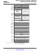
Table 2-2. Terminal Functions
(1)
(continued)
TERMINAL
I/O/Z DESCRIPTION
PT DA
NAME
PIN # PIN #
GPIO7 42 10 I/O/Z General-purpose input/output 7
EPWM4B O Enhanced PWM4 output B
SCIRXDA I SCI-A receive data
– –
GPIO12 47 13 I/O/Z General-purpose input/output 12
TZ1 I Trip Zone input 1
SCITXDA O SCI-A transmit data
– –
GPIO16 27 35 I/O/Z General-purpose input/output 16
SPISIMOA I/O SPI slave in, master out
– –
TZ2 I Trip Zone input 2
GPIO17 26 34 I/O/Z General-purpose input/output 17
SPISOMIA I/O SPI-A slave out, master in
– –
TZ3 I Trip zone input 3
GPIO18 24 32 I/O/Z General-purpose input/output 18
SPICLKA I/O SPI-A clock input/output
SCITXDA O SCI-A transmit
Output clock derived from SYSCLKOUT. XCLKOUT is either the same frequency,
one-half the frequency, or one-fourth the frequency of SYSCLKOUT. This is controlled
by bits 1:0 (XCLKOUTDIV) in the XCLK register. At reset, XCLKOUT =
XCLKOUT O/Z
SYSCLKOUT/4. The XCLKOUT signal can be turned off by setting XCLKOUTDIV
to 3. The mux control for GPIO18 must also be set to XCLKOUT for this signal to
propogate to the pin.
GPIO19 25 33 I/O/Z General-purpose input/output 19
External Oscillator Input. The path from this pin to the clock block is not gated by the
XCLKIN mux function of this pin. Care must be taken not to enable this path for clocking if it is
being used for the other periperhal functions
SPISTEA I/O SPI-A slave transmit enable input/output
SCIRXDA I SCI-A receive
ECAP1 I/O Enhanced Capture input/output 1
GPIO28 48 14 I/O/Z General-purpose input/output 28
SCIRXDA I SCI receive data
SDAA I/OD I
2
C data open-drain bidirectional port
TZ2 I Trip zone input 2
GPIO29 1 15 I/O/Z General-purpose input/output 29.
SCITXDA O SCI transmit data
SCLA I/OD I
2
C clock open-drain bidirectional port
TZ3 I Trip zone input 3
GPIO32 31 – I/O/Z General-purpose input/output 32
SDAA I/OD I
2
C data open-drain bidirectional port
EPWMSYNCI I Enhanced PWM external sync pulse input
ADCSOCAO O ADC start-of-conversion A
Copyright © 2008–2013, Texas Instruments Incorporated Introduction 13
Submit Documentation Feedback
Product Folder Links: TMS320F28027 TMS320F28026 TMS320F28023 TMS320F28022 TMS320F28021
TMS320F28020 TMS320F280200