
Datasheet
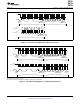


Frame1Two-WireSlaveAddressByte
Frame2PointerRegisterByte
1
StartBy
Master
ACKBy
TMP421/22/23
ACKBy
TMP421/22/23
1 9 1
Frame3DataByte1
ACKBy
TMP421/22/23
1
D7
SDA
(Continued)
SCL
(Continued)
D6 D5 D4 D3 D2 D1 D0
9
9
SDA
SCL
0 0 1 1 0 0
(1)
R/
W P7 P6 P5 P4 P3 P2 P1 P0
¼
¼
StopBy
Master
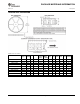
Frame1Two-WireSlaveAddressByte Frame2PointerRegisterByte
1
StartBy
Master
ACKBy
TMP421/22/23
ACKBy
TMP421/22/23
Frame3Two-WireSlaveAddressByte Frame4DataByte1ReadRegister
StartBy
Master
ACKBy
TMP421/22/23
NACKBy
Master
(2)
From
TMP421/22/23
1 9 1
9
1 9 1
9
SDA
SCL
0 0 1 R/
W P7 P6 P5 P4 P3 P2 P1 P0
¼
¼
¼
¼
SDA
(Continued)
SCL
(Continued)
1 0 0 1
1 0 0
(1)
1 0 0
(1)
R/
W D7 D6 D5 D4 D3 D2 D1 D0
TMP421
TMP422
TMP423
www.ti.com
SBOS398C –JULY 2007–REVISED MAY 2012
(1) Slave address 1001100 shown.
Figure 17. Two-Wire Timing Diagram for Write Word Format
(1) Slave address 1001100 shown.
(2) Master should leave SDA high to terminate a single-byte read operation.
Figure 18. Two-Wire Timing Diagram for Single-Byte Read Format
Copyright © 2007–2012, Texas Instruments Incorporated Submit Documentation Feedback 21
Product Folder Link(s): TMP421 TMP422 TMP423