
Datasheet


TMP411-Q1
SBOS527F –DECEMBER 2010–REVISED NOVEMBER 2013
www.ti.com
RESOLUTION REGISTER CONVERSION RATE REGISTER
The RES1 and RES0 bits (resolution bits 1 and 0) of The Conversion Rate Register controls the rate at
the Resolution Register set the resolution of the local which temperature conversions are performed. This
temperature measurement channel. Remote register adjusts the idle time between conversions but
temperature measurement channel resolution is not not the conversion timing itself, thereby allowing the
affected. Changing the local channel resolution also TMP411-Q1 power dissipation to be balanced with
affects the conversion time and rate of the TMP411- the temperature register update rate. Table 8 shows
Q1. The Resolution Register is set by writing to the conversion rate options and corresponding
pointer address 1Ah and is read by reading from current consumption.
pointer address 1Ah. Table 7 shows the resolution
bits for the Resolution Register. ONE-SHOT CONVERSION
When the TMP411-Q1 is in shutdown mode (SD = 1
Table 7. Resolution Register: Local Channel
in the Configuration Register), a single conversion on
Programmable Resolution
both channels is started by writing any value to the
RESOLUTION REGISTER (Read = 1Ah, Write = 1Ah, POR =
One-Shot Start Register, pointer address 0Fh. This
1Ch)
write operation starts one conversion; the TMP411-
CONVERSION
Q1 returns to shutdown mode when that conversion
RES1 RES0 RESOLUTION TIME
completes. The value of the data sent in the write
(Typical)
command is irrelevant and is not stored by the
0 0 9 bits (0.5°C) 12.5 ms
TMP411-Q1. When the TMP411-Q1 is in shutdown
10 bits
mode, an initial 200 μs is required before a one-shot
0 1 25 ms
(0.25°C)
command can be given. (NOTE: When a shutdown
11 bits
command is issued, the TMP411-Q1 completes the
1 0 50 ms
(0.125°C)
current conversion before shutting down.) This wait
12 bits 100 ms
time only applies to the 200 μs immediately following
1 1
(0.0625°C)
shutdown. One-shot commands can be issued
without delay thereafter.
Bits 2 through 4 of the Resolution Register must
always be set to 1. Bits 5 through 7 of the Resolution
Register must always be set to 0. The power-on-reset
value of this register is 1Ch.
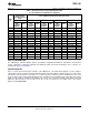
Table 8. Conversion Rate Register
CONVERSION RATE REGISTER (Read = 04h, Write = 0Ah, POR = 08h)
AVERAGE IQ (TYP) (μA)
CONVERSION/SE
R7 R6 R5 R4 R3 R2 R1 R0
C
V
S
= 2.7V V
S
= 5.5V
0 0 0 0 0 0 0 0 0.0625 11 32
0 0 0 0 0 0 0 1 0.125 17 38
0 0 0 0 0 0 1 0 0.25 28 49
0 0 0 0 0 0 1 1 0.5 47 69
0 0 0 0 0 1 0 0 1 80 103
0 0 0 0 0 1 0 1 2 128 155
0 0 0 0 0 1 1 0 4 190 220
07h to 0Fh 8 373 413
18 Submit Documentation Feedback Copyright © 2010–2013, Texas Instruments Incorporated
Product Folder Links: TMP411-Q1