
Datasheet


Data Valid
22
SPISIMO
SPISOMI
SPICLK
(clock polarity = 1)
SPICLK
(clock polarity = 0)
SPISIMO Data
Must Be Valid
SPISOMI Data Is Valid
21
12
18
17
14
13
SPISTE
(A)
F28M36P63C, F28M36P53C, F28M36H53C, F28M36H53B, F28M36H33C, F28M36H33B
www.ti.com
SPRS825C –OCTOBER 2012–REVISED FEBRUARY 2014
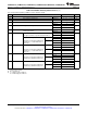
Table 7-43. SPI Slave Mode External Timing (Clock Phase = 1)
(1) (2) (3) (4)
NO. MIN MAX UNIT
12 t
c(SPC)S
Cycle time, SPICLK 8t
c(LCO)
ns
13 t
w(SPCH)S
Pulse duration, SPICLK high (clock polarity = 0) 0.5t
c(SPC)S
– 10 0.5t
c(SPC)S
ns
t
w(SPCL)S
Pulse duration, SPICLK low (clock polarity = 1) 0.5t
c(SPC)S
– 10 0.5t
c(SPC)S
14 t
w(SPCL)S
Pulse duration, SPICLK low (clock polarity = 0) 0.5t
c(SPC)S
– 10 0.5t
c(SPC)S
ns
t
w(SPCH)S
Pulse duration, SPICLK high (clock polarity = 1) 0.5t
c(SPC)S
– 10 0.5t
c(SPC)S
17 t
su(SOMI-SPCH)S
Setup time, SPISOMI before SPICLK high (clock polarity = 0) 0.125t
c(SPC)S
ns
t
su(SOMI-SPCL)S
Setup time, SPISOMI before SPICLK low (clock polarity = 1) 0.125t
c(SPC)S
18 t
v(SPCL-SOMI)S
Valid time, SPISOMI data valid after SPICLK low 0.75t
c(SPC)S
ns
(clock polarity = 1)
t
v(SPCH-SOMI)S
Valid time, SPISOMI data valid after SPICLK high 0.75t
c(SPC)S
(clock polarity = 0)
21 t
su(SIMO-SPCH)S
Setup time, SPISIMO before SPICLK high (clock polarity = 0) 35 ns
t
su(SIMO-SPCL)S
Setup time, SPISIMO before SPICLK low (clock polarity = 1) 35
22 t
v(SPCH-SIMO)S
Valid time, SPISIMO data valid after SPICLK high 0.5t
c(SPC)S
– 10 ns
(clock polarity = 0)
t
v(SPCL-SIMO)S
Valid time, SPISIMO data valid after SPICLK low 0.5t
c(SPC)S
– 10
(clock polarity = 1)
(1) The MASTER / SLAVE bit (SPICTL.2) is cleared and the CLOCK PHASE bit (SPICTL.3) is cleared.
(2) t
c(SPC)
= SPI clock cycle time = LSPCLK/4 or LSPCLK/(SPIBRR + 1)
(3) Internal clock prescalers must be adjusted such that the SPI clock speed is limited to the following SPI clock rate:
Master mode transmit 25-MHz MAX, master mode receive 12.5-MHz MAX
Slave mode transmit 12.5-MHz MAX, slave mode receive 12.5-MHz MAX.
(4) The active edge of the SPICLK signal referenced is controlled by the CLOCK POLARITY bit (SPICCR.6).
A. In the slave mode, the SPISTE signal should be asserted low at least 0.5t
c(SPC)
before the valid SPI clock edge and
remain low for at least 0.5t
c(SPC)
after the receiving edge (SPICLK) of the last data bit.
Figure 7-45. SPI Slave Mode External Timing (Clock Phase = 1)
Copyright © 2012–2014, Texas Instruments Incorporated Peripheral Information and Timings 235
Submit Documentation Feedback
Product Folder Links: F28M36P63C F28M36P53C F28M36H53C F28M36H53B F28M36H33C F28M36H33B