
Datasheet


Settling Time (ns)
0
100
200
300
400
500
600
700
800
900
1000
1100
0 50 100 150 200 250 300 350 400 450 500
DAC Step Size (Codes)
15 Codes 7 Codes 3 Codes 1 Code
DAC Accuracy
F28M36P63C, F28M36P53C, F28M36H53C, F28M36H53B, F28M36H33C, F28M36H33B
SPRS825C –OCTOBER 2012–REVISED FEBRUARY 2014
www.ti.com
7.1.2.1 On-Chip Comparator and DAC Electrical Data and Timing
Table 7-3. Electrical Characteristics of the Comparator/DAC
over recommended operating conditions (unless otherwise noted)
CHARACTERISTIC MIN TYP MAX UNITS
Comparator
Comparator Input Range V
SSA
– V
DDA
V
Comparator response time to PWM Trip Zone (Async) 30 ns
Input Offset ±5 mV
Input Hysteresis
(1)
35 mV
DAC
DAC Output Range V
SSA
– V
DDA
V
DAC resolution 10 bits
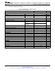
DAC settling time See Figure 7-5
DAC Gain –1.5 %
DAC Offset 10 mV
Monotonic Yes
INL ±3 LSB
(1) Hysteresis on the comparator inputs is achieved with a Schmidt trigger configuration. This results in an effective 100-kΩ feedback
resistance between the output of the comparator and the non-inverting input of the comparator.
Figure 7-5. DAC Settling Time
160 Peripheral Information and Timings Copyright © 2012–2014, Texas Instruments Incorporated
Submit Documentation Feedback
Product Folder Links: F28M36P63C F28M36P53C F28M36H53C F28M36H53B F28M36H33C F28M36H33B