
Datasheet


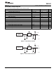


V
ID+
20%
V
ID
3.3V
2.8V
V
ID(pp)
V
OD(pp)
V
ID–
V
OD
20%
80% 80%
0V
t
PHL
t
PLH
t
f
t
r
T0391-01
50%
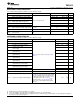
V
OL
t
sk(D)
V
Y
V
Z
V
OH
V
OC
DV
OC(SS)
T0392-01
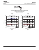
T0424-01
t
clk1
t
clk2
V
CD(PP)
V
OD(PP)
TMDSoutputs
HiZduringthisduration
ValidInput TMDS clock
thatmeetsthemin
Frequency Thresholdand
Amplitude
TMDSoutputclockwith
peaktopeakswing
complianttotheHDMI
specandsamefrequency
astheInput TMDSclock
frequency
TMDS
outputs
HiZ
TMDS361B
www.ti.com
SLLS988A –SEPTEMBER 2009– REVISED JULY 2011
Figure 10. TMDS Main-Link Timing Measurements
Figure 11. Definition of Intra-Pair Differential Skew
Figure 12. TMDS Main-Link Common-Mode Measurements
Figure 13. Clock-Detect Timing Diagram
Copyright © 2009–2011, Texas Instruments Incorporated 17