
Datasheet


www.ti.com
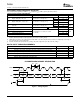
ABSOLUTE MAXIMUM RATINGS
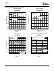
DISSIPATION RATING TABLE
TLV5638
SLAS225C – JUNE 1999 – REVISED JANUARY 2004
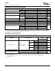
Terminal Functions
TERMINAL
I/O/P DESCRIPTION
NAME NO.
AGND 5 P Ground
CS 3 I Chip select. Digital input active low, used to enable/disable inputs
DIN 1 I Digital serial data input
OUT A 4 O DAC A analog voltage output
OUT B 7 O DAC B analog voltage output
REF 6 I/O Analog reference voltage input/output
SCLK 2 I Digital serial clock input
V
DD
8 P Positive power supply
over operating free-air temperature range (unless otherwise noted)
(1)
UNIT
Supply voltage (V
DD
to AGND) 7 V
Reference input voltage range -0.3 V to V
DD
+ 0.3 V
Digital input voltage range -0.3 V to V
DD
+ 0.3 V
Operating free-air temperature range, T
A
TLV5638C 0°C to 70°C
TLV5638I -40°C to 85°C
TLV5638Q -40°C to 125°C
TLV5638M -55°C to 125°C
Storage temperature range, T
stg
-65°C to 150°C
Lead temperature 1,6 mm (1/16 inch) from case for 10 seconds 260°C
(1) Stresses beyond those listed under, , absolute maximum ratings” may cause permanent damage to the device. These are stress ratings
only, and functional operation of the device at these or any other conditions beyond those indicated under, , recommended operating
conditions” is not implied. Exposure to absolute-maximum-rated conditions for extended periods may affect device reliability.
T
A
≤ 25°C DERATING FACTOR T
A
= 70°C T
A
= 85°C T
A
= 125°C
PACKAGE
POWER RATING ABOVE T
A
= 25°C
(1)
POWER RATING POWER RATING POWER RATING
D 635 mW 5.08 mW/°C 407 mW 330 mW 127 mW
FK 1375 mW 11.00 mW/°C 880 mW 715 mW 275 mW
JG 1050 mW 8.40 mW/°C 672 mW 546 mW 210 mW
(1) This is the inverse of the traditional Junction-to-Ambient thermal Resistance (R θ
JA
). Thermal Resistances are not production tested and
are for informational purposes only.
3