
Datasheet


SERIAL CLOCK FREQUENCY AND UPDATE RATE
f
sclkmax
+
1
t
whmin
) t
wlmin
+ 30 MHz
(2)
f
updatemax
+
1
16
ǒ
t
whmin
) t
wlmin
Ǔ
+ 1.95 MHz
(3)
DATA FORMAT
TLV5608
TLV5610
TLV5629
SLAS268G – MAY 2000 – REVISED NOVEMBER 2008 ....................................................................................................................................................
www.ti.com
Difference between DSP mode (MODE = N.C. or 0) and µ C (MODE = 1) mode:
• In µ C mode, FS needs to be held low until all 16 data bits have been transferred. If FS is driven high before
the 16th falling clock edge, the data transfer is cancelled. The DAC is updated after a rising edge on FS.
• In DSP mode, FS needs to stay low for 20 ns and can go high before the 16th falling clock edge.
• In DSP mode there needs to be one falling SCLK edge before FS goes low to start the write (DIN) cycle. This
extra falling SCLK edge has to happen at least 5 ns before FS goes low, t
su(CK-FS)
≥ 5 ns.
• In µ C mode, the extra falling SCLK edge is not necessary. However, if it does happen, the extra negative
SCLK edge is not allowed to occur within 10 ns after FS goes HIGH to finish the WRITE cycle (t
su(FS-C17)
).
The maximum serial clock frequency is given by:
The maximum update rate is:
Note, that the maximum update rate is just a theoretical value for the serial interface, as the settling time of the
DAC has to be considered also.
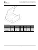
The 16-bit data word consists of two parts:
• Address bits (D150D12)
• Data bits (D110D0)
D15 D14 D13 D12 D11 D10 D9 D8 D7 D6 D5 D4 D3 D2 D1 D0
A3 A2 A1 A0 DATA
Register Map
A3 A2 A1 A0 FUNCTION
0 0 0 0 DAC A
0 0 0 1 DAC B
0 0 1 0 DAC C
0 0 1 1 DAC D
0 1 0 0 DAC E
0 1 0 1 DAC F
0 1 1 0 DAC G
0 1 1 1 DAC H
1 0 0 0 CTRL0
1 0 0 1 CTRL1
1 0 1 0 Preset
1 0 1 1 Reserved
1 1 0 0 DAC A and B
1 1 0 1 DAC C and D
1 1 1 0 DAC E and F
1 1 1 1 DAC G and H
12 Submit Documentation Feedback Copyright © 2000 – 2008, Texas Instruments Incorporated
Product Folder Link(s): TLV5608 TLV5610 TLV5629