
Datasheet


TLV5604
2.7-V TO 5.5-V 10-BIT 3-µS QUADRUPLE DIGITAL-TO-ANALOG CONVERTERS
WITH POWER DOWN
SLAS176B – DECEMBER 1997 – REVISED JULY 2002
7
POST OFFICE BOX 655303 • DALLAS, TEXAS 75265
electrical characteristics over recommended operating free-air temperature range
(unless otherwise noted) (continued)
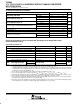
digital input timing requirements
MIN NOM MAX UNIT
t
su(CS–FS)
Setup time, CS low before FS↓ 10 ns
t
su(FS–CK)
Setup time, FS low before first negative SCLK edge 8 ns
t
su(C16–FS)
Setup time, sixteenth negative SCLK edge after FS low on which bit D0 is sampled before
rising edge of FS
10 ns
t
su(C16–CS)
Setup time. The first positive SCLK edge after D0 is sampled before CS rising edge. If FS
is used instead of the SCLK positive edge to update the DAC, then the setup time is between
the FS rising edge and CS rising edge.
10 ns
t
wH
Pulse duration, SCLK high 25 ns
t
wL
Pulse duration, SCLK low 25 ns
t
su(D)
Setup time, data ready before SCLK falling edge 8 ns
t
h(D)
Hold time, data held valid after SCLK falling edge 5 ns
t
wH(FS)
Pulse duration, FS high 20 ns
PARAMETER MEASUREMENT INFORMATION
123451516
D15 D14 D13 D12 D1 D0
t
su(FS-CK)
t
su(CS-FS)
t
wH(FS)
t
h(D)
t
su(D)
t
wH
t
wL
t
su(C16-CS)
t
su(C16-FS)
SCLK
DIN
CS
FS
Figure 1. Timing Diagram