
Datasheet


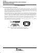


SLOS310B − DECEMBER 2000 − REVISED SEPTEMBER 2006
13
POST OFFICE BOX 655303 • DALLAS, TEXAS 75265
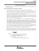
APPLICATION INFORMATION
driving a capacitive load
When the amplifier is used to drive heavy capacitive loads, the device’s phase margin will be reduced which
could lead to high frequency ringing or oscillations. The TLV4120’s high current drive capability reduces this
possibility. However, for capacitive loads of greater than 1 nF, it is suggested that a resistor be placed in series
(R
NULL
) with the output of the amplifier as shown in Figure 22 which should help reduce the ringing.
R
NULL
V
DD
/2
SHDN
−
+
−
+
A1
A2
C
B
R
S
C
S
C
L
R
F
R
NULL
R
L
C
L
NOTE: R
NULL
will reduce the output drive capability of the TLV4120.
Figure 22. Driving a Capacitive Load
offset voltage
The output offset voltage, (V
OO
) is the sum of:
1. The input offset voltage (V
IO
) multiplied by the noninverting gain
2. The noninverting input bias current (I
IB
) multiplied by the resistance on this node multiplied by the
noninverting gain
3. The inverting bias current multiplied by the feedback resistor.
+
−
V
I
R
G
R
BIAS
/2
R
F
I
IB−
V
O
I
IB+
Figure 23. Output Offset Voltage Model