
Datasheet


TLV320DAC3100
www.ti.com
SLAS671A –FEBRUARY 2010–REVISED MAY 2012
6 REGISTER MAP
6.1 TLV320DAC3100 Register Map
All features on this device are addressed using the I
2
C bus. All of the writable registers can be read back.
However, some registers contain status information or data, and are available for reading only.
The TLV320DAC3100 contains several pages of 8-bit registers, and each page can contain up to 128
registers. The register pages are divided up based on functional blocks for this device. The pages defined
for the TLV320DAC3100 are 0, 1, 3, 8–9, 12–13 (DAC coefficient pages). Page 0 is the default home
page after RESET. Page control is done by writing a new page value into register 0 of the current page.
The control registers for the TLV320DAC3100 are described in detail as follows. All registers are 8 bits in
width, with D7 referring to the most-significant bit of each register, and D0 referring to the least-significant
bit.
Pages 0, 1, 3, 8–9, and 12–13 are available for use; however, all other pages and registers are reserved.
Do not read from or write to reserved pages and registers. Also, do not write other than the reset values
for the reserved bits and read-only bits of non-reserved registers; otherwise, device functionality failure
can occur.
Note that the page and register numbers are shown in decimal format. For use in microcode, these
decimal values may require conversion to hexadecimal format. For convienience, the register
numbers are shown in both formats, whereas the page numbers are shown only in decimal format.
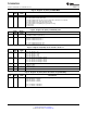
Table 6-1. Summary of Register Map
Page Number Description
0 Page 0 is the default page on power up. Configuration for serial interface, digital I/O, etc.
1 Configuration for DAC, output drivers, volume controls, etc.
Register 16 controls the MCLK divider that controls the interrupt pulse duration, debounce timing, and detection-block
3
clock.
8–9 DAC filter and DRC coefficients (buffer A)
12–13 DAC filter and DRC coefficients (buffer B)
6.2 Control Registers, Page 0 (Default Page): Clock Multipliers, Dividers, Serial
Interfaces, Flags, Interrupts, and GPIOs
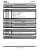
Page 0 / Register 0 (0x00): Page Control Register
READ/ RESET
BIT DESCRIPTION
WRITE VALUE
D7–D0 R/W 0000 0000 0000 0000: Page 0 selected
0000 0001: Page 1 selected
...
1111 1110: Page 254 selected
1111 1111: Page 255 selected
Page 0 / Register 1 (0x01): Software Reset
READ/ RESET
BIT DESCRIPTION
WRITE VALUE
D7–D1 R/W 0000 000 Reserved. Write only zeros to these bits.
D0 R/W 0 0: Don't care
1: Self-clearing software reset for control register
Page 0 / Register 2 (0x02): Reserved
READ/ RESET
BIT DESCRIPTION
WRITE VALUE
D7–D0 R XXXX XXXX Reserved. Do not write to this register.
Copyright © 2010–2012, Texas Instruments Incorporated REGISTER MAP 61
Submit Documentation Feedback
Product Folder Link(s): TLV320DAC3100