
Datasheet


TLV320AIC33
SLAS480B – JANUARY 2006 – REVISED DECEMBER 2008 ...........................................................................................................................................
www.ti.com
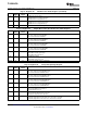
Page 0 / Register 98: GPIO1 Control Register (continued)
BIT READ/ RESET DESCRIPTION
WRITE VALUE
D2 R/W 0 GPIO1 Interrupt Duration Control
0: GPIO1 Interrupt occurs as a single active-high pulse of typical duration 2ms.
1: GPIO1 Interrupt occurs as continuous pulses until the Interrupt Flags register (register 96) is read by
the host
D1 R 0 GPIO1 General Purpose Input Value
0: A logic-low level is input to GPIO1
1: A logic-high level is input to GPIO1
D0 R/W 0 GPIO1 General Purpose Output Value
0: GPIO1 outputs a logic-low level
1: GPIO1 outputs a logic-high level
Page 0 / Register 99: GPIO2 Control Register
BIT READ/ RESET DESCRIPTION
WRITE VALUE
D7-D4 R/W 0000 GPIO2 Output Control
0000: GPIO2 is disabled
0001: Reserved. Do not use.
0010: GPIO2 output = jack/headset detect interrupt (interrupt polarity: active high. Typical interrupt
duration: 1.75 ms.)
0011: GPIO2 = general purpose input
0100: GPIO2 = general purpose output
0101-0111: GPIO2 input = digital microphone input, data sampled on clock rising and falling edges
1000: GPIO2 = bit clock for audio serial data bus (programmable as input or output)
1001: GPIO2 output = Headset Detect OR Button Press Interrupt
1010: GPIO2 output = Headset Detect OR Button Press OR Short-Circuit Detect OR AGC Noise
Detect Interrupt
1011: GPIO2 output = Short Circuit Detect OR AGC Noise Detect Interrupt
1100: GPIO2 output = Headset Detect OR Button Press OR Short-Circuit Detect Interrupt
1101: GPIO2 output = Short Circuit Detect Interrupt
1110: GPIO2 output = AGC Noise Detect Interrupt
1111: GPIO2 output = Button Press / Hookswitch Interrupt
D3 R/W 0 GPIO2 General Purpose Output Value
0: GPIO1 outputs a logic-low level
1: GPIO1 outputs a logic-high level
D2 R 0 GPIO2 General Purpose Input Value
0: A logic-low level is input to GPIO2
1: A logic-high level is input to GPIO2
D1 R/W 0 GPIO2 Interrupt Duration Control
0: GPIO2 Interrupt occurs as a single active-high pulse of typical duration 2ms.
1: GPIO2 Interrupt occurs as continuous pulses until the Interrupt Flags register (register 96) is read by
the host
D0 R/W 0 Reserved. Write only zero to this register bit.
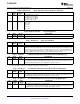
Page 0 / Register 100: Additional GPIO Control Register A
BIT READ/ RESET DESCRIPTION
WRITE VALUE
D7-D6 R/W 00 SDA Pin Control
(1)
The SDA pin hardware includes pull-down capability only (open-drain NMOS), so an external pull-up
resistor is required when using this pin, even in GPIO mode.
00: SDA pin is not used as general purpose I/O
01: SDA pin used as general purpose input
10: SDA pin used as general purpose output
11: Reserved. Do not write this sequence to these register bits.
D5 R/W 0 SDA General Purpose Output Control
(1)
0: SDA driven to logic-low when used as general purpose output
1: SDA driven to logic-high when used as general purpose output (requires external pull-up resistor)
(1) The control bits in Register 100 are only valid in SPI Mode, when SELECT=1.
74 Submit Documentation Feedback Copyright © 2006 – 2008, Texas Instruments Incorporated
Product Folder Link(s): TLV320AIC33