
Datasheet


N-1 N-2 1 0 N-1 N-2 1 0
word
clock
bit clock
data
in/out
RightChannelData
RightChannelData
LeftChannelData
LeftChannelData
N-1 N-2 1 0 N-1 N-2 1 0
word
clock
bit clock
data
in/out
DSP Mode
LeftJustifiedMode
offset
offset
offset
AUDIO DATA CONVERTERS
AUDIO CLOCK GENERATION
TLV320AIC33
www.ti.com
........................................................................................................................................... SLAS480B – JANUARY 2006 – REVISED DECEMBER 2008
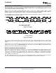
Figure 26. DSP Mode and Left Justified Modes, Showing the
Effect of a Programmed Data Word Offset
The TLV320AIC33 supports the following standard audio sampling rates: 8 kHz, 11.025 kHz, 12 kHz, 16 kHz,
22.05 kHz, 24 kHz, 32 kHz, 44.1 kHz, 48 kHz, 88.2 kHz, and 96 kHz. The converters can also operate at
different sampling rates in various combinations, which are described further below.
The data converters are based on the concept of an Fsref rate that is used internal to the part, and it is related to
the actual sampling rates of the converters through a series of ratios. For typical sampling rates, Fsref will be
either 44.1 kHz or 48 kHz, although it can realistically be set over a wider range of rates up to 53 kHz, with
additional restrictions applying if the PLL is used. This concept is used to set the sampling rates of the ADC and
DAC, and also to enable high quality playback of low sampling rate data, without high frequency audible noise
being generated.
The sampling rate of the ADC and DAC can be set to Fsref/NDAC or 2 × Fsref/NDAC, with NDAC being 1, 1.5, 2,
2.5, 3, 3.5, 4, 4.5, 5, 5.5, or 6.
While only one Fsref can be used at a time in the part, the ADC and DAC sampling rates can differ from each
other by using different NADC and NDAC divider ratios for each. For example, with Fsref=44.1-kHz, the DAC
sampling rate can be set to 44.1-kHz by using NDAC=1, while the ADC sampling rate can be set to 8.018-kHz by
using NADC=5.5.
When the ADCs and DACs are operating at different sampling rates, an additional word clock is required, to
provide information regarding where data begins for the ADC versus the DAC. In this case, the standard bit clock
signal (which can be supplied through the BCLK pin or through GPIO2) is used to transfer both ADC and DAC
data, the standard word clock signal is used to identify the start of the DAC data, and a separate ADC word clock
signal (denoted ADWK) is used. This clock can be supplied or generated from GPIO1 at the same time the DAC
word clock is supplied or generated from WCLK.
The audio converters in the TLV320AIC33 need an internal audio master clock at a frequency of 256 × Fsref,
which can be obtained in a variety of manners from an external clock signal applied to the device.
A more detailed diagram of the audio clock section of the TLV320AIC33 is shown in Figure 27 .
Copyright © 2006 – 2008, Texas Instruments Incorporated Submit Documentation Feedback 27
Product Folder Link(s): TLV320AIC33