
Datasheet


T0146-08
WCLK
BCLK
DOUT
DIN
t (WS)
h
t (WS)
h
t (BCLK)
L
t (DO-BCLK)
d
t
r
t
f
t (DI)
S
t (BCLK)
H
t (DI)
h
t (WS)
S
t (WS)
S
TLV320AIC3110
SLAS647B –DECEMBER 2009–REVISED MAY 2012
www.ti.com
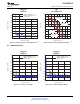
3.4.4 DSP Timing in Slave Mode
All specifications at 25°C, DVDD = 1.8 V
Note: All timing specifications are measured at characterization.
IOVDD = 1.1 V IOVDD = 3.3 V
PARAMETER UNITS
MIN MAX MIN MAX
t
H
(BCLK) BCLK high period 35 35 ns
t
L
(BCLK) BCLK low period 35 35 ns
t
s
(WS) WCLK setup 8 8 ns
t
h
(WS) WCLK hold 8 8 ns
t
d
(DO-BCLK) BCLK to DOUT delay 45 20 ns
t
s
(DI) DIN setup 8 8 ns
t
h
(DI) DIN hold 8 8 ns
t
r
Rise time 4 4 ns
t
f
Fall time 4 4 ns
Figure 3-4. DSP Timing in Slave Mode
12 ELECTRICAL SPECIFICATIONS Copyright © 2009–2012, Texas Instruments Incorporated
Submit Documentation Feedback
Product Folder Links: TLV320AIC3110