
Datasheet


ABSOLUTE MAXIMUM RATINGS
PACKAGE THERMAL RATINGS
(1)
SYSTEM THERMAL CHARACTERISTICS - TLV320AIC3106IRGZ
(1)
DISSIPATION RATINGS FOR BGA PACKAGES
(1)
TLV320AIC3106
SLAS509E – DECEMBER 2006 – REVISED DECEMBER 2008 ........................................................................................................................................
www.ti.com
over operating free-air temperature range (unless otherwise noted)
(1) (2)
VALUE UNIT
AVDD_DAC to AVSS_DAC, DRVDD to DRVSS, AVSS_ADC – 0.3 to 3.9 V
AVDD to DRVSS – 0.3 to 3.9 V
IOVDD to DVSS – 0.3 to 3.9 V
DVDD to DVSS – 0.3 to 2.5 V
AVDD_DAC to DRVDD – 0.1 to 0.1 V
Digital input voltage to DVSS – 0.3 to IOVDD + 0.3 V
Analog input voltage to AVSS_ADC – 0.3 to AVDD + 0.3 V
Operating temperature range – 40 to 85 ° C
Storage temperature range – 65 to 105 ° C
T
J
Max Junction temperature 105 ° C
Power dissipation (T
J
Max – T
A
)/ θ
JA
Thermal impedance , BGA package 63 ° C/W
θ
JA
Thermal impedance, QFN package — ° C/W
(1) Stresses beyond those listed under absolute maximum ratings may cause permanent damage to the device. These are stress ratings
only, and functional operation of the device at these or any other conditions beyond those indicated under recommended operating
conditions is not implied. Exposure to absolute-maximum-rated conditions for extended periods may affect device reliability.
(2) ESD complicance tested to EIA/JESD22-A114-B and passed.
PARAMETER
R
θ JP
(1)
(C/W) 3.5
Ψ
JT
(2)
( ° C/W) 2
R
θ JA
(3)
(C/W) 24
R
θ JA
(4)
(C/W) 85
(1) R
θ JP
is the internal thermal resistance from junction to the thermal pad. It is required to limit the power dissipation within the device to
500 mW in all cases, including temperatures below 25 ° C. The TLV320AIC3106IRGZ must be soldered down to the copper (ground
plane) under the device to meet the thermal requirements.
(2) Ψ
JT
is defined by the following formula: Ψ
JT
= [T (Junction) – T (Center of top of the case)]/(Total power)
(3) Thermal resistance on a JEDEC high-K board with no airflow. See the JESD 51 standard for a detailed description.
(4) Thermal resistance on a JEDEC low-K board with no airflow. See the JESD 51 standard for a detailed description.
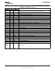
Power Rating at 25 ° C, mW Power Rating, mW Derating Factor, ° C/W
High-K Board 500 500 at 80 ° C 33
Low-K Board 500 500 at 30 ° C 104
(1) It is required to limit the power dissipation within the package to 500 mW in all cases, including temperatures below 25 ° C. This data is
based on using a JEDEC standard four-layer 3-in. × 3-in. (7.62-mm × 7.62-mm) PCB with 2-oz. (0.071-mm thick) trace and copper pad
that is soldered directly to the device.
T
A
= 25 ° C DERATING T
A
= 75 ° C T
A
= 85 ° C
PACKAGE TYPE
POWER RATING FACTOR POWER RATING POWER RATING
BGA 1.27 W 15.9 mW/ ° C 476 mW 317 mW
(1) This data is based on using a JEDEC standard four-layer 3-in. × 3-in. (7.62-mm × 7.62-mm) PCB with 2-oz. (0.071-mm thick) trace and
copper pad that is soldered directly to the device.
6 Submit Documentation Feedback Copyright © 2006 – 2008, Texas Instruments Incorporated
Product Folder Link(s): TLV320AIC3106