
Datasheet


RA(6) RA(5) RA(0) Don’tCare
7-bitRegister Address
Read 8-bitRegisterData
SS
SCLK
MOSI
MISO
Hi-Z Hi-Z
D(7) D(6) D(0)
Hi-Z Hi-Z
SPI COMMUNICATION PROTOCOL
TLV320AIC3106
SLAS509E – DECEMBER 2006 – REVISED DECEMBER 2008 ........................................................................................................................................
www.ti.com
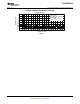
Figure 15. SPI Read
In the SPI control mode, the TLV320AIC3106 uses the pins MFP0=SSB, MFP1=SCLK, MFP2=MISO,
MFP3=MOSI as a standard SPI port with clock polarity setting of 0 (typical microprocessor SPI control bit CPOL
= 0). The SPI port allows full-duplex, synchronous, serial communication between a host processor (the master)
and peripheral devices (slaves). The SPI master (in this case, the host processor) generates the synchronizing
clock (driven onto SCLK) and initiates transmissions. The SPI slave devices (such as the TLV320AIC3106)
depend on a master to start and synchronize transmissions.
A transmission begins when initiated by an SPI master. The byte from the SPI master begins shifting in on the
slave MOSI pin under the control of the master serial clock (driven onto SCLK). As the byte shifts in on the MOSI
pin, a byte shifts out on the MISO pin to the master shift register.
The TLV320AIC3106 interface is designed so that with a clock phase bit setting of 1 (typical microprocessor SPI
control bit CPHA = 1), the master begins driving its MOSI pin and the slave begins driving its MISO pin on the
first serial clock edge. The SSB pin can remain low between transmissions; however, the TLV320AIC3106 only
interprets the first 8 bits transmitted after the falling edge of SSB as a command byte, and the next 8 bits as a
data byte only if writing to a register. Reserved register bits should be written to their default values.
The TLV320AIC3106 is entirely controlled by registers. Reading and writing these registers is accomplished by
the use of an 8-bit command, which is sent to the MOSI pin of the part prior to the data for that register. The
command is constructed as shown in Table X. The first 7 bits specify the register address which is being written
or read, from 0 to 127 (decimal). The command word ends with an R/W bit, which specifies the direction of data
flow on the serial bus. In the case of a register write, the R/W bit should be set to 0. A second byte of data is
sent to the MOSI pin and contains the data to be written to the register.
Reading of registers is accomplished in similar fashion. The 8-bit command word sends the 7-bit register
address, followed by R/W bit = 1 to signify a register read is occurring,. The 8-bit register data is then clocked out
of the part on the MISO pin during the second 8 SCLK clocks in the frame.
Command Word
Bit 7 Bit 6 Bit 5 Bit 4 Bit 3 Bit 2 Bit 1 Bit 0
ADDR6 ADDR5 ADDR4 ADDR3 ADDR2 ADDR1 ADDR0 R/ W
The register map of the TLV320AIC3106 actually consists of multiple pages of registers, with each page
containing 128 registers. The register at address zero on each page is used as a page-control register, and
writing to this register determines the active page for the device. All subsequent read/write operations will access
the page that is active at the time, unless a register write is performed to change the active page. Only two
pages of registers are implemented in this product, with the active page defaulting to page 0 upon device reset.
For example, at device reset, the active page defaults to page 0, and thus all register read/write operations for
addresses 1 to 127 will access registers in page 0. If registers on page 1 must be accessed, the user must write
the 8-bit sequence 0x01 to register 0, the page control register, to change the active page from page 0 to page 1.
20 Submit Documentation Feedback Copyright © 2006 – 2008, Texas Instruments Incorporated
Product Folder Link(s): TLV320AIC3106