
Datasheet


LD(n) LD(n+1)
2 1
0
3
2 1
0
3 3
RD(n)
LEFT CHANNEL RIGHT CHANNEL
LD(n) = nth Sample of Left-Channel Data RD(n) = nth Sample of Right-Channel Data
WORD
CLOCK
BIT
CLOCK
DATA
n-1 n-2
n-3
n-1 n-2
n-3
n-1 n-2
n-3
Ch_Offset_1 = 0 Ch_Offset_1 = 0
LD(n) LD(n+1)
4
3
2
5
1
0
4
3
2
5
1
0
5
RD(n)
LEFT CHANNEL RIGHT CHANNEL
LD(n) = nth Sample of Left-Channel Data RD(n) = nth Sample of Right-Channel Data
WORD
CLOCK
BIT
CLOCK
DATA
n-1 n-1 n-1
Ch_Offset_1 = 2 Ch_Offset_1 = 2
LD(n) LD(n+1)
2 1
0
3
2 1
0
3 3
RD(n)
LEFT CHANNEL RIGHT CHANNEL
LD(n) = nth Sample of Left-Channel Data RD(n) = nth Sample of Right-Channel Data
WORD
CLOCK
BIT
CLOCK
DATA
n-1 n-2
n-3
n-1 n-2
n-3
n-1 n-2
n-3
Ch_Offset_1 = 0 Ch_Offset_1 = 0
DSP Mode
TLV320ADC3101
www.ti.com
...................................................................................................................................... SLAS553A – NOVEMBER 2008 – REVISED SEPTEMBER 2009
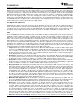
Figure 23. I
2
S Mode (Standard Timing)
Figure 24 shows the I
2
S mode timing with Ch_Offset_1 = 2.
Figure 24. I
2
S Mode With Ch_Offset_1 = 2
Figure 25 shows the I
2
S mode timing with Ch_Offset_1 = 0 and bit clock inverted.
Figure 25. I
2
S Mode With Ch_Offset_1 = 0, Bit Clock Inverted
For I
2
S mode, the number of bit clocks per channel should be greater than or equal to the programmed word
length of the data. Also the programmed offset value should be less than the number of bit clocks per frame by
at least the programmed word length of the data.
In DSP mode, the rising edge of the word clock starts the data transfer with the left-channel data first and is
immediately followed by the right-channel data. Each data bit is valid on the falling edge of the bit clock.
Figure 26 shows the standard timing for the DSP mode.
Copyright © 2008 – 2009, Texas Instruments Incorporated Submit Documentation Feedback 21
Product Folder Link(s) :TLV320ADC3101