
Datasheet


Right-Justified Mode
BCLK
WCLK
DIN/
DOUT
n-1 n-2 1 00 n-1 n-2 1 0
1/fs
LSBMSB
LeftChannel RightChannel
n-3 2 2n-3
LSBMSB
Left-Justified Mode
LD(n)
LD(n+1)
WORD
CLOCK
BIT
CLOCK
DATA
RD(n)
LEFT CHANNEL RIGHT CHANNEL
LD(n) = nth Sample of Left-Channel Data RD(n) = nth Sample of Right-Channel Data
2 1 03 2 1 03
n-3
n-1 n-2 n-3n-1 n-2
n-3n-1 n-2
2 1
0
LD(n) LD(n+1)
3
2 1
0
3
RD(n)
LEFT CHANNEL RIGHT CHANNEL
LD(n) = nth Sample of Left-Channel Data RD(n) = nth Sample of Right-Channel Data
WORD
CLOCK
BIT
CLOCK
DATA
n-1 n-2
n-3
n-1 n-2
n-3
n-1 n-2
n-3
Ch_Offset_1 = 1
Ch_Offset_1 = 1
TLV320ADC3101
SLAS553A – NOVEMBER 2008 – REVISED SEPTEMBER 2009 ......................................................................................................................................
www.ti.com
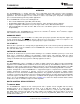
In right-justified mode, the LSB of the left channel is valid on the rising edge of the bit clock preceding the falling
edge of word clock. Similarly, the LSB of the right channel is valid on the rising edge of the bit clock preceding
the rising edge of the word clock. See Figure 16 for right-justifed mode timing.
Figure 16. Timing Diagram for Right-Justified Mode
For right-justified mode, the number of bit clocks per frame should be greater than twice the programmed
word-length of the data. Note that the time-slot-based mode is not available in the right-justified mode.
In left-justified mode, the MSB of the right channel is valid on the rising edge of the bit clock following the falling
edge of the word clock. Similarly, the MSB of the left channel is valid on the rising edge of the bit clock following
the rising edge of the word clock. Figure 17 shows the standard timing of the left-justified mode.
Figure 17. Left-Justified Mode (Standard Timing)
Figure 18 shows the left-justified mode with Ch_Offset_1 = 1.
Figure 18. Left-Justified Mode With Ch_Offset_1 = 1
18 Submit Documentation Feedback Copyright © 2008 – 2009, Texas Instruments Incorporated
Product Folder Link(s) :TLV320ADC3101