
Datasheet


+V
+5 V
CC
R
100 k
LOAD
W
V
O
R3
1 MW
R2
1 MW
R1
1 MW
V
IN
V
A
5 V
0 V
1.67 V 3.33 V
V
A2
V
A1
V
IN
V
O
High
+V
CC
V
O
Low
+V
CC
V
A1
R1
R2
R3
V
A2
R1
R2
R3
D -V = V V
A A1 A2
V = V
A2 CC
´
R2 || R3
R1 + (R2 || R3)
V = V
A1 CC
´
R2
(R1 || R3) + R2
TLV3201
TLV3202
SBOS561A –MARCH 2012–REVISED JUNE 2012
www.ti.com
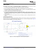
Inverting Comparator With Hysteresis
The inverting comparator with hysteresis requires a three-resistor network that is referenced to the comparator
supply voltage (V
CC
), as shown in Figure 28. When V
IN
at the inverting input is less than V
A
, the output voltage is
high (for simplicity assume V
O
switches as high as V
CC
). The three network resistors can be represented as R1 ||
R3 in series with R2. The lower input trip voltage (V
A1
) is defined by Equation 1:
(1)
When V
IN
is greater than [V
A
× (V
IN
> V
A
)], the output voltage is low, very close to ground. In this case, the three
network resistors can be presented as R2 || R3 in series with R1. The upper trip voltage (V
A2
) is defined by
Equation 2:
(2)
The total hysteresis provided by the network is defined by Equation 3:
(3)
Figure 28. TLV3201 in Inverting Configuration with Hysteresis
12 Submit Documentation Feedback Copyright © 2012, Texas Instruments Incorporated
Product Folder Link(s): TLV3201 TLV3202