
Datasheet


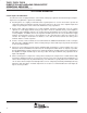


µ
SLOS351D − MARCH 2001 − REVISED FEBRUARY 2004
12
WWW.TI.COM
TYPICAL CHARACTERISTICS
Figure 23
0.00
0.05
0.10
0.0 0.5 1.0 1.5 2.0 2.5 3.0 3.5 4.0 4.5
0.00
0.05
0.10
INVERTING SMALL-SIGNAL RESPONSE
V
DD
= 5 V
A
V
= V
I
= −1
R
L
= 2 kΩ
C
L
= 10 pF
V
I
= 100 mV
pp
T
A
= 25°C
V
O
− Output Voltage − VV
O
V
I
− Input Voltage − VV
I
t − Time − µs
Figure 24
−140
−120
−100
−80
−60
−40
−20
0
10 100 1 k 10 k 100 k
CROSSTALK
vs
FREQUENCY
f − Frequency − Hz
V
DD
= 2.7, 5, & 15 V
V
I
= 1 V
DD
/2
A
V
= 1
R
L
= 2 kΩ
T
A
= 25°C
Crosstalk − dB
Crosstalk
APPLICATION INFORMATION
driving a capacitive load
When the amplifier is configured in this manner, capacitive loading directly on the output decreases the device’s
phase margin leading to high frequency ringing or oscillations. Therefore, for capacitive loads of greater than
10 pF, it is recommended that a resistor be placed in series (R
NULL
) with the output of the amplifier, as shown
in Figure 25. A minimum value of 20 Ω should work well for most applications.
C
LOAD
R
F
Input
Output
R
G
R
NULL
+
−
V
DD
/2
Figure 25. Driving a Capacitive Load