
Datasheet


www.ti.com
T
J
= +150°C
4
3
2
0
−55 −40 −10 20 35
Maximum Power Dissipation − W
5
6
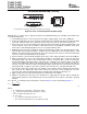
MAXIMUM POWER DISSIPATION
vs
FREE-AIR TEMPERATURE
7
65 95 125
1
T
A
− Free-Air Temperature − °C
DGN Package
Low-K Test PCB
θ
JA
= 52.3°C/W
SOT-23 Package
Low-K Test PCB
θ
JA
= 324°C/W
−25 5 50 80 110
PWP Package
Low-K Test PCB
θ
JA
= 29.7°C/W
SOIC Package
Low-K Test PCB
θ
JA
= 176°C/W
PDIP Package
Low-K Test PCB
θ
JA
= 104°C/W
TLV2470 , , TLV2471
TLV2472 , TLV2473
TLV2474 , TLV2475 , TLV247xA
SLOS232E – JUNE 1999 – REVISED JULY 2007
APPLICATION INFORMATION (continued)
Results are obtained with no air flow and using JEDEC Standard Low-K test PCB.
Figure 47. Maximum Power Dissipation vs Free-Air Temperature
The next consideration is the package constraints. The two sources of heat within an amplifier are quiescent
power and output power. The designer should never forget about the quiescent heat generated within the
device, especially multi-amplifier devices. Because these devices have linear output stages (Class A-B), most of
the heat dissipation is at low output voltages with high output currents. Figure 48 to Figure 53 show this effect,
along with the quiescent heat, with an ambient air temperature of +70 ° C and +125 ° C. When using V
DD
= 3V,
there is generally not a heat problem with an ambient air temperature of +70 ° C. But, when using V
DD
= 5V, the
package is severely limited in the amount of heat it can dissipate. The other key factor when looking at these
graphs is how the devices are mounted on the PCB. The PowerPAD devices are extremely useful for heat
dissipation. But the device should always be soldered to a copper plane to fully use the heat dissipation
properties of the PowerPAD. The SOIC package, on the other hand, is highly dependent on how it is mounted
on the PCB. As more trace and copper area is placed around the device, θ
JA
decreases and the heat dissipation
capability increases. The currents and voltages shown in these graphs are for the total package. For the dual or
quad amplifier packages, the sum of the RMS output currents and voltages should be used to choose the proper
package.
19
Submit Documentation Feedback