
Datasheet


TLV2432, TLV2432A, TLV2434, TLV2434A
Advanced LinCMOS RAIL-TO-RAIL OUTPUT
WIDE-INPUT-VOLTAGE OPERATIONAL AMPLIFIERS
SLOS168F – NOVEMBER 1996 – REVISED MARCH 2001
9
POST OFFICE BOX 655303 • DALLAS, TEXAS 75265
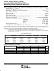
electrical characteristics at specified free-air temperature, V
DD
= 5 V (unless otherwise noted)
PARAMETER
TEST CONDITIONS
T
†
TLV243x
UNIT
PARAMETER
TEST
CONDITIONS
T
A
†
MIN TYP MAX
UNIT
V
IC
=0
TLV243x
25°C 300 2000
V
IO
In
p
ut offset voltage
V
IC
=
0
,
V
O
= 0,
TLV243x
Full range 2500
µV
V
IO
Input
offset
voltage
O
,
V
DD
± = ±2.5 V,
R50Ω
TLV243xA
25°C 300 950
µ
V
R
S
= 50 Ω
TLV243xA
Full range 1500
α
VIO
Tem
p
erature coefficient of in
p
ut offset voltage
25°C
2
µV/°C
α
VIO
Temperature
coefficient
of
input
offset
voltage
to 70°C
2
µ
V/°C
Input offset voltage long-term drift
(see Note 4)
V
IC
=
0,
V
DD
±
=
±2.5 V,
25°C 0.003 µV/mo
I
IO
In
p
ut offset current
V
IC
=
0
,
V
O
= 0,
V
DD
±
=
±2
.
5
V
,
R
S
= 50 Ω
25°C
0.5 60
p
A
I
IO
Input
offset
current
Full range 150
pA
I
IB
In
p
ut bias current
25°C 1 60
p
A
I
IB
Input
bias
current
Full range 150
pA
V
ICR
Common mode in
p
ut voltage range
|V
IO
| ≤ 5mV
R
S
=50Ω
25°C
0
to
4.5
–0.25
to
4.75
V
V
ICR
Common
-
mode
input
voltage
range
|V
IO
|
≤
5
mV
,
R
S
=
50
Ω
Full range
0
to
4.2
V
I
OH
= –100 µA 25°C 4.97
V
OH
High-level output voltage
I
OH
= 5mA
25°C 4 4.35
V
I
OH
= –
5
mA
Full range 4
V
IC
= 2.5 V, I
OL
= 100 µA 25°C 0.01
V
OL
Low-level output voltage
V
IC
=25V
I
OL
=5 A
25°C 0.8
V
V
IC
=
2
.
5
V
,
I
OL
=
5
A
Full range 1.25
V25V
R2kΩ
‡
25°C 2.5 3.8
A
VD
Large-signal differential voltage amplification
V
IC
= 2.5 V,
V
O
=1Vto4V
R
L
=
2
kΩ
‡
Full range 1.5
V/mV
VD
gg g
V
O
=
1
V
to
4
V
R
L
= 1 MΩ
‡
25°C 950
r
i(d)
Differential input resistance 25°C
1000
GΩ
r
i(c)
Common-mode input resistance 25°C
1000
GΩ
c
i(c)
Common-mode input capacitance f = 10 kHz 25°C 8 pF
z
o
Closed-loop output impedance f = 100 kHz, A
V
= 10 25°C 130 Ω
CMRR
Common mode rejection ratio
V
IC
= 0 to 4.5 V, V
O
= 2.5 V,
25°C 70 90
dB
CMRR
Common
-
mode
rejection
ratio
IC
,
O
,
R
S
= 50 Ω
Full range 70
dB
k
SVR
Su
pp
ly voltage rejection ratio (∆V
DD
/∆V
IO
)
V
DD
= 4.4 V to 8 V,
25°C 80 95
dB
k
SVR
Supply
-
voltage
rejection
ratio
(∆V
DD
/∆V
IO
)
DD
,
V
IC
= V
DD
/2, No load
Full range 80
dB
I
DD
Su
pp
ly current (
p
er channel)
V
O
=25V
No load
25°C 100 125
µA
I
DD
Supply
current
(per
channel)
V
O
=
2
.
5
V
,
No
load
Full range 125
µ
A
†
Full range for the C suffix is 0°C to 70°C. Full range for the dual I suffix is – 40°C to 85°C. Full range for the quad I suffix is – 40°C to 125°C.
‡
Referenced to 2.5 V
NOTE 4: Typical values are based on the input offset voltage shift observed through 500 hours of operating life test at T
A
= 150°C extrapolated
to T
A
= 25°C using the Arrhenius equation and assuming an activation energy of 0.96 eV.