
Datasheet


SLAS072E − DECEMBER 1992 − REVISED JANUARY 2004
16
WWW.TI.COM
APPLICATION INFORMATION
1000000000
0111111111
0000000010
0000000001
0000000000
1111111110
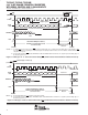
0 0.0096 2.4528 2.4576 2.4624
Digital Output Code
1000000001
1111111101
1111111111
4.9056 4.9104 4.9152
512
511
2
1
0
1022
Step
513
1021
1023
0.0024
V
I
− Analog Input Voltage − V
V
ZT
= V
ZS
+ 1/2 LSB
V
ZS
See Notes A and B
4.9080
0.0048
V
FT
= V
FS
− 1/2 LSB
V
FS
NOTES: A. This curve is based on the assumption that V
ref+
and V
ref−
have been adjusted so that the voltage at the transition from digital
0 to 1 (V
ZT
) is 0.0024 V and the transition to full scale (V
FT
) is 4.908 V. 1 LSB = 4.8 mV.
B. The full-scale value (V
FS
) is the step whose nominal midstep value has the highest absolute value. The zero-scale value (V
ZS
)
is the step whose nominal midstep value equals zero.
Figure 15. Ideal Conversion Characteristics
Processor
Control
Circuit
Analog
Inputs
A0
A1
A2
A3
A4
A5
A6
A7
A8
A9
A10
I/O CLOCK
CS
ADDRESS
DATA OUT
EOC
REF+
REF−
GND
TLV1543
To Source
Ground
3-V DC Regulated
1
2
3
4
5
6
7
8
9
11
12
15
18
17
16
19
14
13
10
Figure 16. Serial Interface