
Datasheet


TLC7701, TLC7725, TLC7703
TLC7733, TLC7705
SLVS087M –DECEMBER 1994–REVISED MARCH 2012
www.ti.com
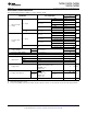
ELECTRICAL CHARACTERISTICS
over recommended operating conditions
(1)
(unless otherwise noted)
TLC77xx
PARAMETER TEST CONDITIONS UNIT
MIN TYP MAX
V
DD
= 2 V 1.8
I
OH
= –20 µA V
DD
= 2.7 V 2.5
High-level output
V
OH
V
voltage
V
DD
= 4.5 V 4.3
I
OH
= 2 –mA V
DD
= 4.5 V 3.7
V
DD
= 2 V 0.2
I
OL
= 20 µA V
DD
= 2.7 V 0.2
Low-Level output
V
OL
V
voltage
V
DD
= 4.5 V 0.2
I
OL
= 2 mA V
DD
= 4.5 V 0.5
TCLC7701 1.04 1.1 1.16
TLC7725 2.18 2.25 2.32
Negative-going input threshold voltage,
V
IT–
TLC7703 V
DD
= 2 V to 6 V 2.56 2.63 2.70 mV
SENSE
(2)
TLC7733 2.86 2.93 3
TLC7705 4.47 4.55 4.63
TCLC7701 30
TLC7725
V
hus
Hysteresis voltage, SENSE TLC7703 V
DD
= 2 V to 6 V mV
70
TLC7733
TLC7705
V
res
Power-up reset voltage
(3)
I
OL
= 20 µA 1 V
RESIN V
I
= 0 V to V
DD
2
CONTROL V
I
= V
DD
7 15
I
I
Input current µA
SENSE V
I
= 5 V 5 10
SENSE, TLC7701 only V
I
= 5 V 2
RESIN = V
DD
, SENSE = V
DD
≥ V
IT
max + 0.2 V,
I
DD
Supply current 9 16 µA
CONTROL = 0 V, Outputs open
VDD = 5 V, V
CT
= 0,
I
DD(d)
Supply current during t
d
RESIN = V
DD
, SENSE = V
DD
, 120 150 µA
CONTROL = 0 V, Outputs open
C
I
Input capacitance, SENSE V
I
= 0 V to V
DD
50 pF
(1) All characteristics are measured with C
T
= 0.1 µF.
(2) To ensure best stability of the threshold voltage, a bypass capacitor (ceramic, 0.1 mF) should be connected near the supply terminals.
(3) The lowest supply voltage at which RESET becomes active. The symbol V
res
is not currently listed within EIA or JEDEC standards for
semiconductor symbology. Rise time of V
DD
≥ 15 µs/V.
6 Submit Documentation Feedback Copyright © 1994–2012, Texas Instruments Incorporated
Product Folder Link(s): TLC7701, TLC7725, TLC7703 TLC7733, TLC7705