
Datasheet


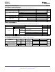


1
10
CLR
CLK
20
2
19
D1
D
Q_
CK
R
V
CC
Y1
3
18
D2
D
Q_
CK
R
Y2
4
17
D3
D
Q_
CK
R
Y3
5
16
D4
D
Q_
CK
R
Y4
6
15
D5
D
Q_
CK
R
Y5
7
14
D6
D
Q_
CK
R
Y6
8
13
D7
D
Q_
CK
R
Y7
12
D
Q_
CK
R
Y8
9
D8
11
GND
TLC59213
TLC59213A
SLVS867A –MAY 2009–REVISED MARCH 2010
www.ti.com
FUNCTION TABLE
(EACH LATCH)
(1)
INPUTS OUTPUT
Y
CLR CLK D
L X X Z (OFF)
H ↑ L Z (OFF)
H ↑ H H (ON)
H L X Y
0
H ↓ X Y
0
(1) L: Low-level
H: High-level
X: Irrelevant
↑: Rising edge
↓: Falling edge
Z : High-impedance (off)
BLOCK DIAGRAM
ABSOLUTE MAXIMUM RATINGS
(1)
over operating free-air temperature range (unless otherwise noted)
MIN MAX UNIT
V
DD
Supply voltage range –0.5 15 V
V
I
Input voltage range –0.5 V
CC
+ 0.5 V
Collector-emitter voltage –0.5 15 V
I
O
Peak output current –500 mA
I
IK
Input clamp current V
I
< 0 V –20 mA
I
OK
Output clamp current V
O
< 0 V –500 mA
N package 69
q
JA
Package thermal impedance
(2)
°C/W
PW package 83
T
stg
Storage temperature range –65 150 °C
(1) Stresses beyond those listed under "absolute maximum ratings" may cause permanent damage to the device. These are stress ratings
only, and functional operation of the device at these or any other conditions beyond those indicated under "recommended operating
conditions" is not implied. Exposure to absolute-maximum-rated conditions for extended periods may affect device reliability.
(2) The package thermal impedance is calculated in accordance with JESD 51-7.
2 Submit Documentation Feedback Copyright © 2009–2010, Texas Instruments Incorporated
Product Folder Link(s): TLC59213 TLC59213A