
Datasheet


TLC3704, TLC3704M
QUAD MICROPOWER LinCMOS VOLTAGE COMPARATORS
SLCS117C − NOVEMBER 1986 − REVISED NOVEMBER 2009
8
POST OFFICE BOX 655303 • DALLAS, TEXAS 75265
PRINCIPLES OF OPERATION
LinCMOS process
The LinCMOS process is a linear polysilicon-gate CMOS process. Primarily designed for single-supply
applications, LinCMOS products facilitate the design of a wide range of high-performance analog functions from
operational amplifiers to complex mixed-mode converters.
This short guide is intended to answer the most frequently asked questions related to the quality and reliability
of LinCMOS products. Direct further questions to the nearest TI field sales office.
electrostatic discharge
CMOS circuits are prone to gate oxide breakdown when exposed to high voltages even if the exposure is only
for very short periods of time. Electrostatic discharge (ESD) is one of the most common causes of damage to
CMOS devices. It can occur when a device is handled without proper consideration for environmental
electrostatic charges, e.g., during board assembly. If a circuit in which one amplifier from a dual op amp is being
used and the unused pins are left open, high voltages tends to develop. If there is no provision for ESD
protection, these voltages may eventually punch through the gate oxide and cause the device to fail. To prevent
voltage buildup, each pin is protected by internal circuitry.
Standard ESD-protection circuits safely shunt the ESD current by providing a mechanism whereby one or more
transistors break down at voltages higher than the normal operating voltages but lower than the breakdown
voltage of the input gate. This type of protection scheme is limited by leakage currents which flow through the
shunting transistors during normal operation after an ESD voltage has occurred. Although these currents are
small, on the order of tens of nanoamps, CMOS amplifiers are often specified to draw input currents as low as
tens of picoamps.
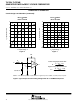
To overcome this limitation, TI design engineers developed the patented ESD-protection circuit shown in
Figure 1. This circuit can withstand several successive 2-kV ESD pulses, while reducing or eliminating leakage
currents that may be drawn through the input pins. A more detailed discussion of the operation of the TI
ESD-protection circuit is presented on the next page.
All input and output pins on LinCMOS and Advanced LinCMOS products have associated ESD-protection
circuitry that undergoes qualification testing to withstand 2000 V discharged from a 100-pF capacitor through
a 1500-Ω resistor (human body model) and 200 V from a 100-pF capacitor with no current-limiting resistor
(charged device model). These tests simulate both operator and machine handling of devices during normal
test and assembly operations.
To Protected Circuit
D3
R2
Q2
D2D1
Q1
Input
GND
R1
V
DD
Figure 1. LinCMOS ESD-Protection Schematic