
Datasheet


TLC3704, TLC3704M
QUAD MICROPOWER LinCMOS VOLTAGE COMPARATORS
SLCS117C − NOVEMBER 1986 − REVISED NOVEMBER 2009
4
POST OFFICE BOX 655303 • DALLAS, TEXAS 75265
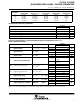
recommended operating conditions
TLC3704I
UNIT
MIN NOM MAX
UNIT
Supply voltage, V
DD
3 5 16 V
Common-mode input voltage, V
IC
− 0.2 V
DD
− 1.5 V
High-level output current, I
OH
− 20 mA
Low-level output current, I
OL
20 mA
Operating free-air temperature, T
A
− 40 85 °C
electrical characteristics at specified operating free-air temperature, V
DD
= 5 V, V
IC
= 0 (unless
otherwise noted)
PARAMETER
TEST CONDITIONS
T
TLC3704I
UNIT
PARAMETER
TEST CONDITIONS
T
A
MIN TYP MAX
UNIT
V
Input offset voltage
V
DD
= 5 V to 10 V, 25°C 1.2 5
mV
V
IO
Input offset voltage
V
IC
= V
ICR
min, See Note 3 −40°C to 85°C 7
mV
I
Input offset current
V 25V
25°C 1 pA
I
IO
Input offset current V
IC
= 2.5 V
85°C 1 nA
I
Input bias current
V 25V
25°C 5 pA
I
IB
Input bias current V
IC
= 2.5 V
85°C 2 nA
V
Common mode input voltage range
25°C
0 to
V
DD
− 1
V
V
ICR
Common-mode input voltage range
−40°C to 85°C
0 to
V
DD
− 1.5
V
25°C 84
CMRR Common-mode rejection ratio V
IC
= V
ICR
min
85°C 84
dB
CMRR
Common mode
rejection
ratio
V
IC
V
ICR
min
−40°C 83
dB
25°C 85
k
SVR
Supply-voltage rejection ratio V
DD
= 5 V to 10 V
85°C 85
dB
k
SVR
Supply voltage
rejection
ratio
V
DD
5
V
to
10
V
−40°C 83
dB
V
High level output voltage
V 1V
I 4mA
25°C 4.5 4.7
V
V
OH
High-level output voltage V
ID
= 1 V, I
OH
= − 4 mA
85°C
4.3
V
V
Low level output voltage
V 1V
I 4mA
25°C 210 300
mV
V
OL
Low-level output voltage V
ID
= −1 V, I
OH
= 4 mA
85°C
400
mV
I
Supply current (all four comparators)
Outputs low
No load
25°C 35 80
µA
I
DD
Supply current (all four comparators) Outputs low, No load
−40°C to 85°C 125
µA
NOTE 3: The offset voltage limits given are the maximum values required to drive the output up to 4.5 V or down to 0.3 V.