
Datasheet


TLC3702
DUAL MICROPOWER LinCMOS™ VOLTAGE COMPARATORS
SLCS013E − NOVEMBER 1986 − REVISED MARCH 2012
13
POST OFFICE BOX 655303 • DALLAS, TEXAS 75265
TYPICAL CHARACTERISTICS
†
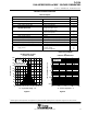
Table of Graphs
FIGURE
V
IO
Input offset voltage Distribution 8
I
IB
Input bias current vs Free-air temperature 9
CMRR Common-mode rejection ratio vs Free-air temperature 10
k
SVR
Supply-voltage rejection ratio vs Free-air temperature 11
V
High level output current
vs Free-air temperature 12
V
OH
High-level output current
vs Free air temperature
vs High-level output current
12
13
V
Low level output voltage
vs Low-level output current 14
V
OL
Low-level output voltage
vs Low level output current
vs Free-air temperature
14
15
t
t
Transition time vs Load capacitance 16
Supply current response vs Time 17
Low-to-high-level output response Low-to-high level output propagation delay time 18
High-to-low level output response High-to-low level output propagation delay time 19
t
PLH
Low-to-high level output propagation delay time vs Supply voltage 20
t
PHL
High-to-low level output propagation delay time vs Supply voltage 21
vs Frequency 22
I
DD
Supply current
vs Frequency
vs Supply voltage
22
23
I
DD
Supply current
vs Supply voltage
vs Free-air temperature
23
24
Figure 8
Number of Units
V
DD
= 5 V
V
IC
= 2.5 V
T
A
= 25° C
−5 −4 −3 −2 − 10 1 2 3 4 5
V
IO
− Input Offset Voltage − mV
DISTRIBUTION OF INPUT
OFFSET VOLTAGE
200
180
160
140
120
100
80
60
40
20
0
698 Units Tested
From 4 Wafer Lots
Figure 9
I
T
A
− Free-Air Temperature − °C
IB
− Input Bias Current − nA
25 50 75 100 125
10
1
0.1
0.01
0.001
INPUT BIAS CURRENT
vs
FREE-AIR TEMPERATURE
V
DD
= 5 V
V
IC
= 2.5 V
†
Data at high and low temperatures are applicable only within the rated operating free-air temperature ranges of the various devices.