
Datasheet


TLC3702
DUAL MICROPOWER LinCMOS™ VOLTAGE COMPARATORS
SLCS013E − NOVEMBER 1986 − REVISED MARCH 2012
11
POST OFFICE BOX 655303 • DALLAS, TEXAS 75265
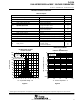
PARAMETER MEASUREMENT INFORMATION
−
+
DUT
V
DD
+
−
−
+
−
+
C2
1 μF
R4
47 kΩ
R5
1.8 kΩ 1%
C3
0.68 μF
IC1c
1/4 TLC274CN
IC1a
1/4 TLC274CN
IC1b
1/4 TLC274CN
R6
1 MΩ
R7
1.8 kΩ 1%
R8
10 kΩ 1%
R1
240 kΩ
R2
10 kΩ
C1
0.1 μF
R3
100 Ω
C4
0.1 μF
Integrator
R9
100 Ω 1%
Buffer
Triangle
Generator
V
IO
(X100)
Figure 6. Circuit for Input Offset Voltage Measurement
Response time is defined as the interval between the application of an input step function and the instant when
the output reaches 50% of its maximum value. Response time for the low-to-high-level output is measured from
the leading edge of the input pulse, while response time for the high-to-low-level output is measured from the
trailing edge of the input pulse. Response time measurement at low input signal levels can be greatly affected
by the input offset voltage. The offset voltage should be balanced by the adjustment at the inverting input as
shown in Figure 7, so that the circuit is just at the transition point. A low signal, for example 105-mV or 5-mV
overdrive, causes the output to change state.