
Datasheet


SLOS051E − OCTOBER 1987 − REVISED AUGUST 2008
29
POST OFFICE BOX 655303 • DALLAS, TEXAS 75265
APPLICATION INFORMATION
−
+
2.5 V
V
O
C
L
−2.5 V
V
I
(a) C
L
= 20 pF, R
L
= NO LOAD
(b) C
L
= 170 pF, R
L
= NO LOAD
(c) C
L
= 190 pF, R
L
= NO LOAD (d) TEST CIRCUIT
T
A
= 25°C
f = 1 kHz
V
I(PP)
= 1 V
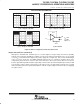
Figure 41. Effect of Capacitive Loads and Test Circuit
output characteristics (continued)
Although the TLC27M2 and TLC27M7 possess excellent high-level output voltage and current capability,
methods for boosting this capability are available, if needed. The simplest method involves the use of a pullup
resistor (R
P
) connected from the output to the positive supply rail (see Figure 42). There are two disadvantages
to the use of this circuit. First, the NMOS pulldown transistor N4 (see equivalent schematic) must sink a
comparatively large amount of current. In this circuit, N4 behaves like a linear resistor with an on-resistance
between approximately 60 Ω and 180 Ω, depending on how hard the operational amplifier input is driven. With
very low values of R
P
, a voltage offset from 0 V at the output occurs. Second, pullup resistor R
P
acts as a drain
load to N4 and the gain of the operational amplifier is reduced at output voltage levels where N5 is not supplying
the output current.