
Datasheet


SLOS092D − SEPTEMBER 1987 − REVISED MARCH 2001
10
POST OFFICE BOX 655303 • DALLAS, TEXAS 75265
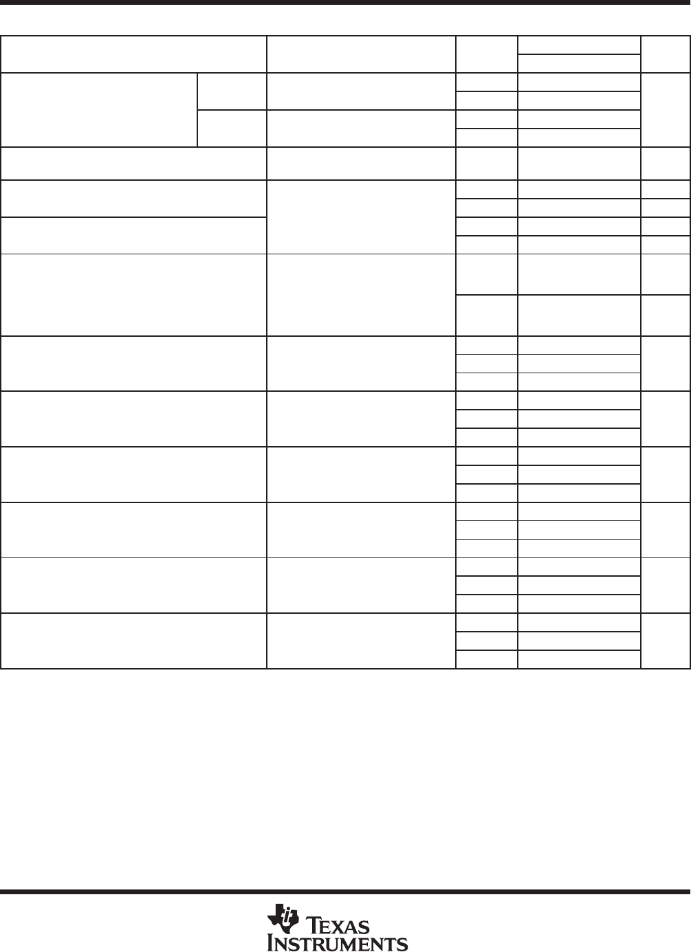
electrical characteristics at specified free-air temperature, V
DD
= 5 V (unless otherwise noted)
PARAMETER
TEST CONDITIONS
T
A
†
TLC274M, TLC279M
UNIT
PARAMETER
TEST CONDITIONS
T
A
†
MIN TYP MAX
UNIT
TLC274M
V
O
= 1.4 V,
V
IC
= 0,
25°C 1.1 10
mV
V
IO
Input offset voltage
TLC274M
V
O
= 1.4 V,
R
S
= 50 Ω,
V
IC
= 0,
R
L
= 10 kΩ
Full range
12
mV
V
IO
Input offset voltage
TLC279M
V
O
= 1.4 V,
V
IC
= 0,
25°C 320 900
V
TLC279M
V
O
= 1.4 V,
R
S
= 50 Ω,
V
IC
= 0,
R
L
= 10 kΩ
Full range
3750
µV
α
VIO
Average temperature coefficient of input
offset voltage
25°C to
125°C
2.1 µV/°C
I
IO
Input offset current (see Note 4)
25°C 0.1 60 pA
I
IO
Input offset current (see Note 4)
V
O
= 2.5 V,
V
IC
= 2.5 V
125°C 1.4 15 nA
I
IB
Input bias current (see Note 4)
V
O
= 2.5 V, V
IC
= 2.5 V
25°C
0.6 60 pA
I
IB
Input bias current (see Note 4)
125°C 9 35 nA
V
ICR
Common-mode input voltage range
25°C
0
to
4
−0.3
to
4.2
V
V
ICR
Common-mode input voltage range
(see Note 5)
Full range
0
to
3.5
V
25°C 3.2 3.8
V
OH
High-level output voltage V
ID
= 100 mV, R
L
= 10 kΩ
−55°C
3 3.8
V
V
OH
High-level output voltage
V
ID
= 100 mV,
R
L
= 10 kΩ
125°C 3 3.8
V
25°C 0 50
V
OL
Low-level output voltage V
ID
= −100 mV, I
OL
= 0
−55°C
0 50
mV
V
OL
Low-level output voltage
V
ID
= −100 mV,
I
OL
= 0
125°C 0 50
mV
Large-signal differential voltage
25°C 5 23
A
VD
Large-signal differential voltage
amplification
V
O
= 0.25 V to 2 V
,
R
L
= 10 kΩ
−55°C
3.5 35
V/mV
A
VD
amplification
V
O
= 0.25 V to 2 V,
R
L
= 10 kΩ
125°C 3.5 16
V/mV
25°C 65 80
CMRR Common-mode rejection ratio V
IC
= V
ICR
min
−55°C 60 81
dB
CMRR
Common-mode rejection ratio
V
IC
= V
ICR
min
125°C 60 84
dB
Supply-voltage rejection ratio
25°C 65 95
k
SVR
Supply-voltage rejection ratio
(∆V
DD
/∆V
IO
)
V
DD
= 5 V to 10 V, V
O
= 1.4 V
−55°C
60 90
dB
k
SVR
(∆V
DD
/∆V
IO
)
V
DD
= 5 V to 10 V,
V
O
= 1.4 V
125°C 60 97
dB
V
O
= 2.5 V,
V
IC
= 2.5 V,
25°C 2.7 6.4
I
DD
Supply current (four amplifiers)
V
O
= 2.5 V,
No load
V
IC
= 2.5 V,
−55°C
4 10
mA
I
DD
Supply current (four amplifiers)
No load
125°C 1.9 4.4
mA
†
Full range is −55°C to 125°C.
NOTES: 4. The typical values of input bias current and input offset current below 5 pA were determined mathematically.
5. This range also applies to each input individually.