
Datasheet


TLC272, TLC272A, TLC272B, TLC272Y, TLC277
LinCMOS PRECISION DUAL OPERATIONAL AMPLIFIERS
SLOS091E – OCTOBER 1987 – REVISED FEBRUARY 2002
19
POST OFFICE BOX 655303 • DALLAS, TEXAS 75265
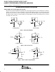
TYPICAL CHARACTERISTICS
Table of Graphs
FIGURE
V
IO
Input offset voltage Distribution 6, 7
α
VIO
Temperature coefficient of input offset voltage Distribution 8, 9
vs Hi
g
h-level output current 10
,
11
V
OH
Hi
g
h-level output volta
g
e
vs
High
-
level
out ut
current
vs Supply voltage
10
,
11
12
V
OH
High level
out ut
voltage
vs
Su ly
voltage
vs Free-air temperature
12
13
vs Common-mode input volta
g
e 14
,
15
V
Low level output voltage
vs
Common
-
mode
in ut
voltage
vs Differential input volta
g
e
14
,
15
16
V
OL
Low-level output voltage
vs
Differential
in ut
voltage
vs Free-air temperature
16
17
vs
Free air
tem erature
vs Low-level output current
17
18, 19
vs Suppl
y
volta
g
e 20
A
VD
Lar
g
e-si
g
nal differential volta
g
e amplification
vs
Su ly
voltage
vs Free-air temperature
20
21
A
VD
Large signal
differential
voltage
am lification
vs
Free air
tem erature
vs Frequency
21
32, 33
I
IB
Input bias current vs Free-air temperature 22
I
IO
Input offset current vs Free-air temperature 22
V
IC
Common-mode input voltage vs Supply voltage 23
I
Supply current
vs Supply volta
g
e 24
I
DD
Supply current
vs
Su ly
voltage
vs Free-air temperature
24
25
SR
Slew rate
vs Suppl
y
volta
g
e 26
SR Slew rate
vs
Su ly
voltage
vs Free-air temperature
26
27
Normalized slew rate vs Free-air temperature 28
V
O(PP)
Maximum peak-to-peak output voltage vs Frequency 29
B
Unity gain bandwidth
vs Free-air temperature 30
B
1
Unity-gain bandwidth
vs
Free air
tem erature
vs Supply voltage
30
31
vs Suppl
y
volta
g
e 34
φ
m
Phase mar
g
in
vs
Su ly
voltage
vs Free-air temperature
34
35
φ
m
Phase
margin
vs
Free air
tem erature
vs Load capacitance
35
36
V
n
Equivalent input noise voltage vs Frequency 37
Phase shift vs Frequency 32, 33