
Datasheet


TLC226x, TLC226xA
Advanced LinCMOS RAIL-TO-RAIL
OPERATIONAL AMPLIFIERS
SLOS177D – FEBRUARY 1997 – REVISED MARCH 2001
12
POST OFFICE BOX 655303 • DALLAS, TEXAS 75265
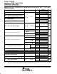
TLC2264C electrical characteristics at specified free-air temperature, V
DD±
= ±5 V (unless
otherwise specified)
PARAMETER
TEST CONDITIONS
T
A
†
TLC2264C
UNIT
PARAMETER
TEST
CONDITIONS
T
A
†
MIN TYP MAX
UNIT
V
IO
In
p
ut offset voltage
25°C 300 2500
µV
V
IO
Input
offset
voltage
Full range 3000
µ
V
α
VIO
Tem
p
erature coefficient of in
p
ut offset voltage
25°C
2
µV/°C
α
VIO
Temperature
coefficient
of
input
offset
voltage
to 70°C
2
µ
V/°C
Input offset voltage long-term drift (see Note 4)
V
IC
= 0,
R
S
=50Ω
V
O
= 0,
25°C
0.003 µV/mo
I
IO
In
p
ut offset current
R
S
=
50
Ω
25°C 0.5
p
A
I
IO
Input
offset
current
Full range 100
pA
I
IB
In
p
ut bias current
25°C 1
p
A
I
IB
Input
bias
current
Full range 100
pA
–5 –5.3
25°C
5
to
5.3
to
V
ICR
Common mode in
p
ut voltage range
|V
IO
|≤5mV
R
S
=50Ω
4 4.2
V
V
ICR
Common
-
mode
input
voltage
range
|V
IO
|
≤5
mV
,
R
S
=
50
Ω
–5
V
Full range
5
to
g
3.5
I
O
= –20 µA 25°C 4.99
I
O
= 100 µA
25°C 4.85 4.94
V
OM+
Maximum positive peak output voltage
I
O
= –
100
µ
A
Full range 4.82
V
I
O
= 400 µA
25°C 4.7 4.85
I
O
= –
400
µ
A
Full range 4.6
V
IC
= 0, I
O
= 50 µA 25°C –4.99
V
IC
=0
I
O
= 500 µA
25°C –4.85 –4.91
V
IC
=
0
,
I
O
=
500
µ
A
Full range –4.85
V
OM–
Maximum negative peak output voltage
V
IC
=0
I
O
=1 A
25°C –4.7 –4.8
V
V
IC
=
0
,
I
O
=
1
A
Full range –4.7
V
IC
=0
I
O
=4 A
25°C –4 –4.3
V
IC
=
0
,
I
O
=
4
A
Full range –3.8
R
L
=50kΩ
25°C 80 200
A
VD
Large-signal differential voltage amplification V
O
= ±4 V
R
L
=
50
kΩ
Full range 55
V/mV
R
L
= 1 MΩ 25°C 1000
r
i(d)
Differential input resistance 25°C
10
12
Ω
r
i(c)
Common-mode input resistance 25°C
10
12
Ω
c
i(c)
Common-mode input capacitance f = 10 kHz, N package 25°C 8 pF
z
o
Closed-loop output impedance f = 100 kHz, A
V
= 10 25°C 220 Ω
CMRR
Common mode rejection ratio
V
IC
= –5 V to 2.7 V, 25°C 75 88
dB
CMRR
Common
-
mode
rejection
ratio
V
O
= 0, R
S
= 50 Ω Full range 75
dB
k
SVR
Su
pp
ly voltage rejection ratio (∆V
DD±
/∆V
IO
)
V
DD±
= ±2.2 V to ±8 V, 25°C 80 95
dB
k
SVR
Supply
-
voltage
rejection
ratio
(∆V
DD±
/∆V
IO
)
V
IC
= 0, No load Full range 80
dB
I
DD
Su
pp
ly current (four am
p
lifiers)
V
O
=0
No load
25°C 0.85 1
mA
I
DD
Supply
current
(four
amplifiers)
V
O
=
0
,
No
load
Full range 1
mA
†
Full range is 0°C to 70°C.
NOTE 4: Typical values are based on the input offset voltage shift observed through 500 hours of operating life test at T
A
= 150°C extrapolated
to T
A
= 25°C using the Arrhenius equation and assuming an activation energy of 0.96 eV.